前言
在多层PCB/封装基板的设计中,会有非常多的过孔连接。低频情况下,过孔不影响信号传输。然而,随着频率上升(GHz级)和信号上升沿变得陡峭(ns级),此时的过孔不能简单地视为电气连接,而必须考虑过孔对信号完整性的影响。本文介绍了三种用于高速信号过孔仿真的方法,借助的工具分别为:HFSS Via Wizard、ADS Via Designer以及HyperLynx LineSim 。
关键词:高速信号,过孔设计,HFSS,ADS,HyperLynx
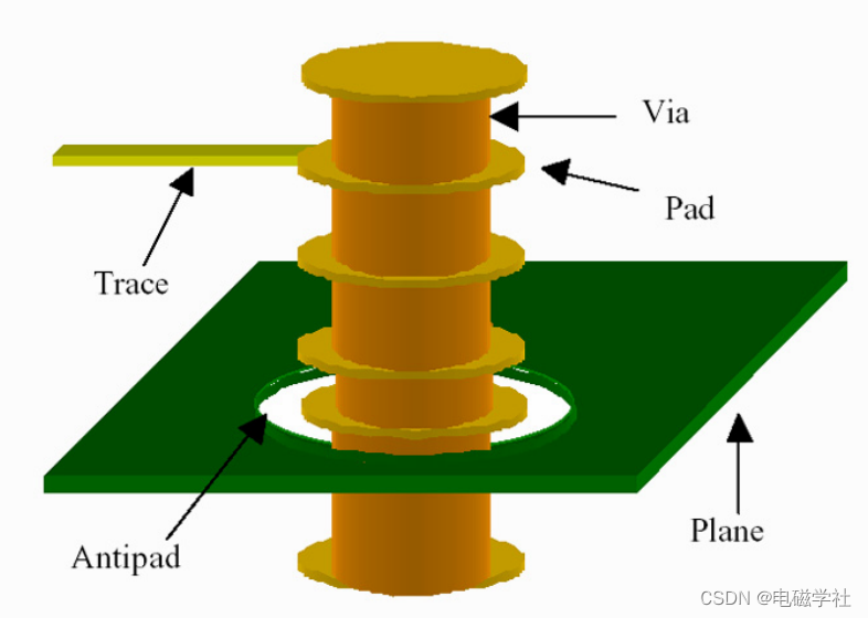
1. 过孔的影响
过孔带来的问题主要集中在寄生电容和寄生电感上。寄生电容会延长信号的上升时间,降低电路的运行速率。寄生电感会削弱旁路电容的作用,降低系统的滤波性能。
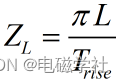
信号延迟主要来自过孔的寄生电容,通过下式计算:
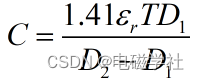
其中,D2为接地焊盘(阻焊区)直径(mm),D1为过孔焊盘直径(mm),T为PCB板厚度(mm),εr为基板介电常数,C为过孔的寄生电容(pF)。
信号的上升时间通过下式计算:
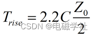
其中,Z0为传输线阻抗,Trise为信号的上升时间(10%-90%)。
过孔的寄生电感,可由下式计算:
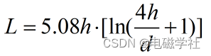
其中,L表示过孔的寄生电感 (nH),h表示过孔的长度 (mm),d表示过孔的直径 (mm)。
由过孔寄生电感引起的等效阻抗变化,可由下式计算:
2. HFSS Via Wizard
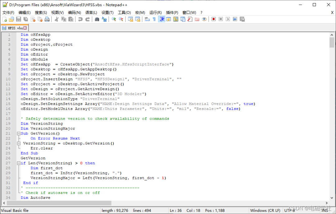
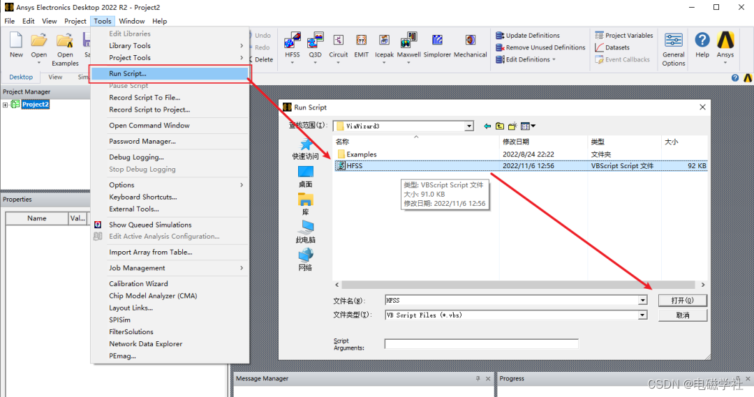
Via Wizard是一款针对HFSS开发的建模小工具,大小只有2MB不到,可以快速生成3D过孔模型。它建模的主要原理是:在该工具的安装路径下生成一个.vbs文件(根据用户在软件UI界面中设置的参数生成),然后HFSS调用该文件去完成建模。了解Ansys自动化建模的同学,听起来是不是很熟悉?讲这个原理的目的是,如果有同学在用Via Wizard这款插件时,遇到无法生成模型的情况,可以在HFSS中手动调用该.vbs文件进行建模。
以下,进行该插件的常规流程演示,可视化操作较为简单,略有删减。
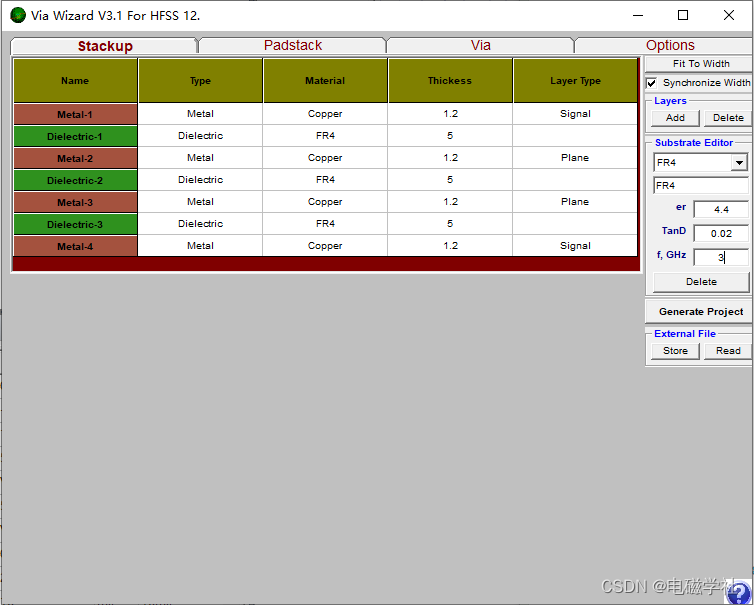
- 设置叠层参数
- 设置信号过孔/地过孔参数
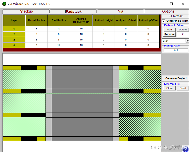
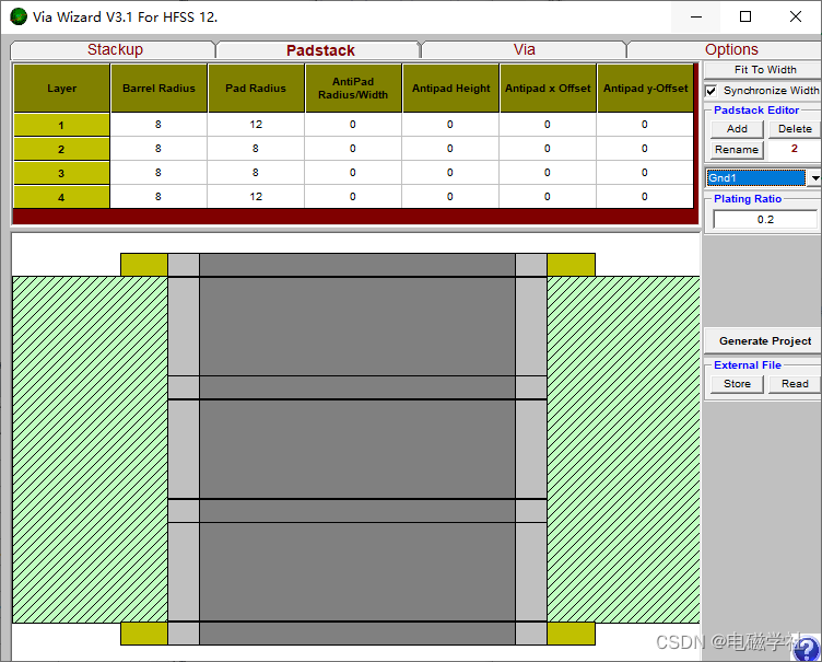
- 设置信号过孔/地过孔的相对位置
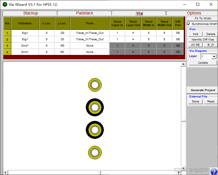
- 在Via Wizard完成设置后,便可Generate生成HFSS中的信号过孔模型。同时该插件还会自动将过孔相关的尺寸设为变量,这样参数化处理之后更方便我们后续对过孔进行优化设计。HFSS中的仿真设置,在此不赘述。
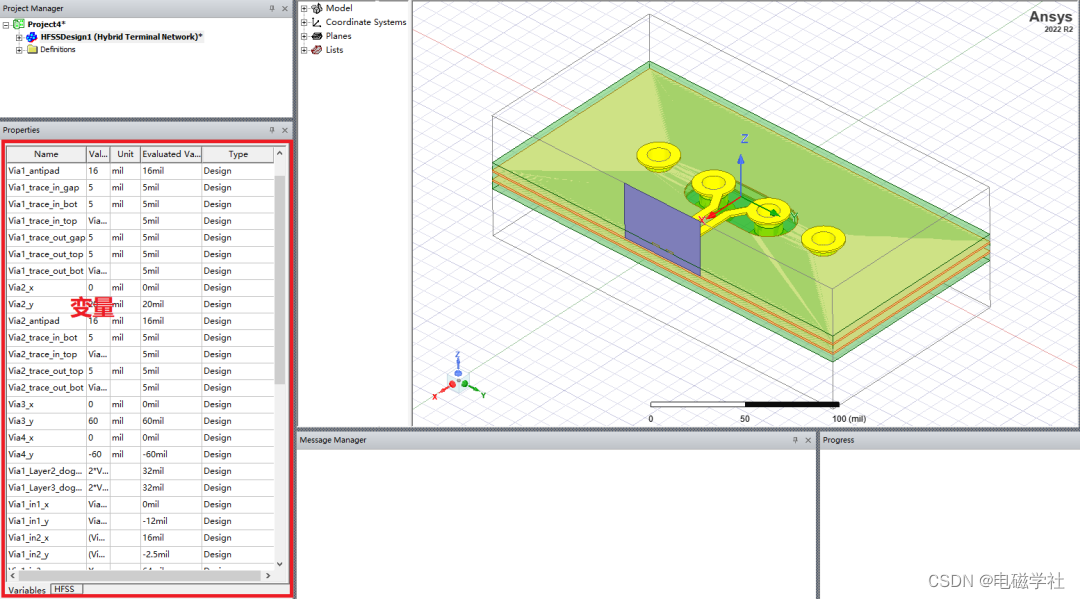
- 仿真时可根据需要进行扫参对比过孔阻抗的变化,各个变量注释如下:
Via(num)_x
The x-location of the via center
Via(num)_y
The y-location of the via center
Via(num)_trace_in_bot
The width of the lower section of the trapezoidal trace into the via
Via(num)_trace_in_top
The width of the upper section of the trapezoidal trace into the via
Via(num)_trace_out_bot
The width of the lower section of the trapezoidal trace out of the via
Via(num)_trace_out_top
The width of the upper section of the trapezoidal trace out of the via
Via(num)_trace_in_bot
The width of the lower section of the trapezoidal trace into the via
Via(num)_backdrill
The depth of copper that is removed from the bottom of the via
Via(num)_in(num)_x
Location of x points for trace into the via
Via(num)_in(num)_y
Location of y points for trace into the via
Via(num)_out(num)_x
Location of x points for trace out of the via
Via(num)_out(num)_y
Location of y points for trace out of the via
For Differential Vias Only
Via(num)_trace_in_gap
The spacing between the differential traces into the via
Via(num)_trace_out_gap
The spacing between the differential traces out of the via
Via(num)_Layer(num)_dogbone
The height of the rectangular clearance between differential vias
Hidden Variables
L(num)_Cond_Thickness
Conductor thickness of that layer
L(num)_Die_Thickness
Dielectric thickness of that layer
L(num)_Cond_Elevation
Elevation in Z-direction of bottom of conductor
L(num)_Die_Elevation
Elevation in Z-direction of bottom of dielectric
Xmin
Minimum X dimensions of project
Xlength
Length of X dimensions of project
Ymin
Minimum Y dimensions of project
Ylength
Length of Y dimensions of project
Zmin
Minimum Z dimensions of project including Airbox
Zlength
Length of Z dimensions of project including Airbox
Via(num)_antipad
This variable is created only if antipads are identical on all layers. This variable will control the antipad dimensions on all layers
Via(num)_Layer(num)_antipad
Antipad radius or width
Via(num)_Layer(num)_antipad_height
Antipad height
Via(num)_Layer(num)_Antipad_x_offset
Antipad registration in X direction
Via(num)_Layer(num)_Antipad_y_offset
Antipad registration in Y direction
Via(num)_Layer(num)_Antipad_xmin
Used as starting point for rectangular antipads. Computed from other variables
Via(num)_Layer(num)_Antipad_ymin
Used as starting point for rectangular antipads. Computed from other variables
Via(num)_Layer(num)_Antipad_x_center
Used as starting point for circular antipads. Computed from other variables
Via(num)_Layer(num)_Antipad_y_center
Used as starting point for circular antipads. Computed from other variables
Via(num)_Layer(num)_Antipad_x_center
Used as starting point for circular antipads. Computed from other variables
Port(num)_in_left_wall
Defines Y location of left edge of WavePortIn
Port(num)_in_right_wall
Defines Y location of right edge of WavePortIn
Port(num)_out_left_wall
Defines Y location of left edge of WavePortOut
Port(num)_out_right_wall
Defines Y location of right edge of WavePortOut
3. ADS Via Designer
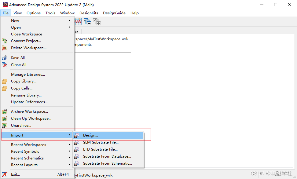
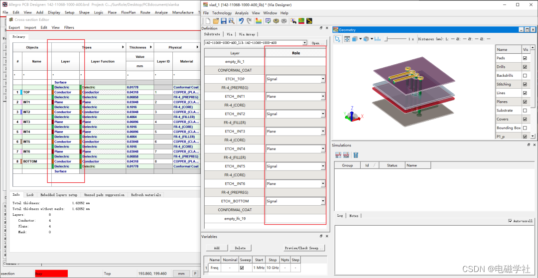
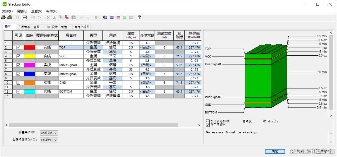
在ADS中进行过孔设计时,如果尚未进行Layout,那么叠层可以自己定义。如果已经有叠层信息了,建议直接将PCB文件导入ADS中,省去建叠层的过程。
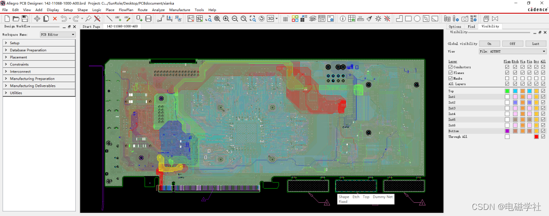
▲本例中使用的NVIDIA显卡PCB文件[2010年产品]
- ADS中导入PCB文件
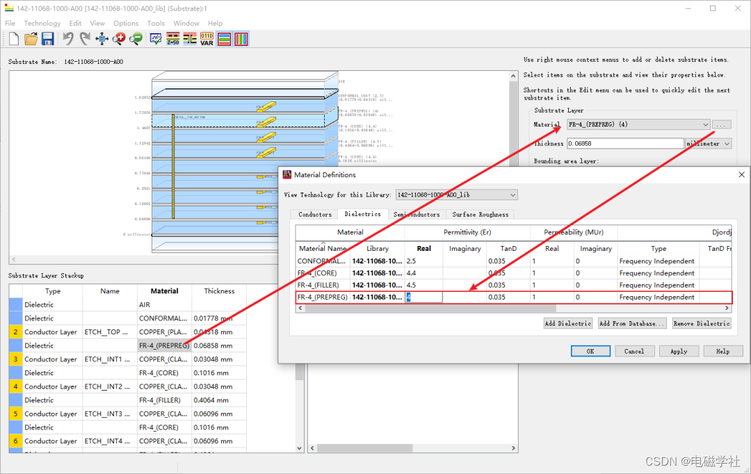
- 叠层信息核对,Dk/Df值应与厂家保持一致。互连工程师会保证自己所画PCB物理尺寸的正确,但一般不会花时间去给你填板材电参数的实际值,这里切记要检查。
- 打开Via Designer,首先根据Allegro PCB的Layer Function修改Via Designer中的Layer Role。
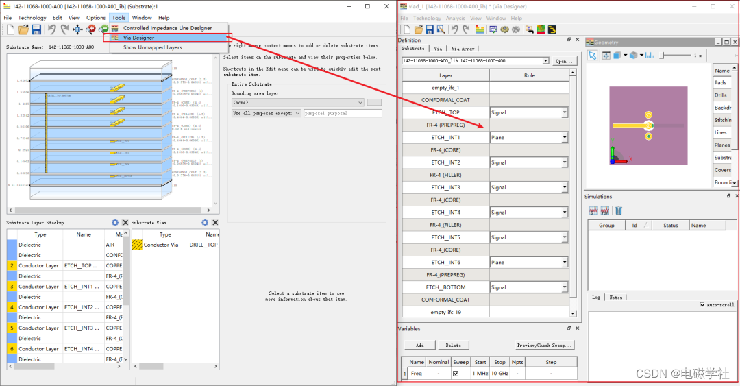
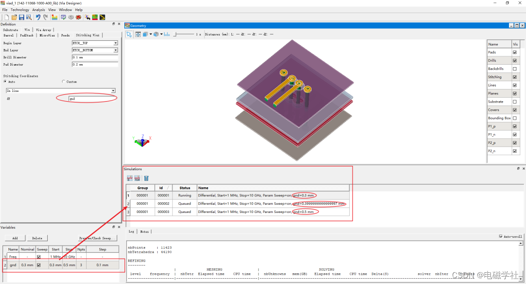
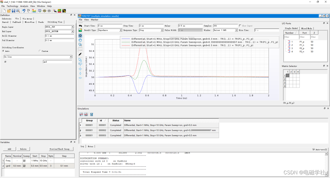
- 同样地,如果要对某个参数进行扫参优化设计,将其设为变量,设置取值范围。我们以地孔(缝合孔)为例,看该参数对结果的影响,将其设为gnd=0.3,0.4,0.5。
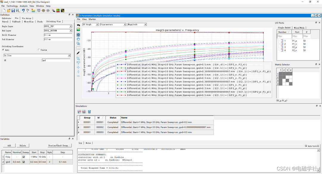
- 不同变量下的仿真结果:单端、差分形式的S参数及TDR阻抗。
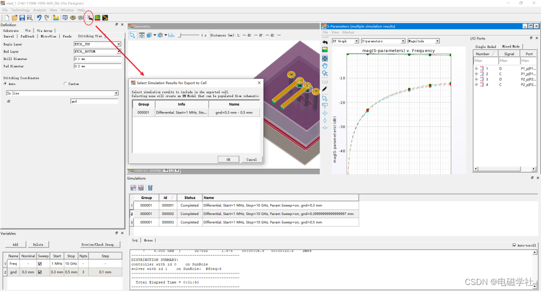
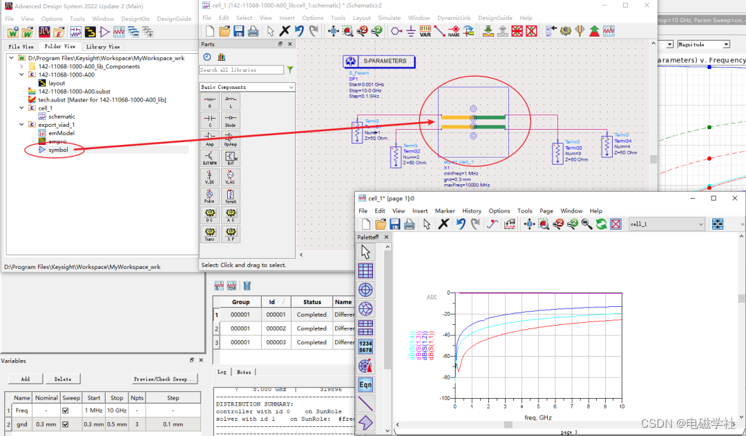
- 建模得到的过孔模型,也可导出至ADS schematic中进行其他的链路仿真
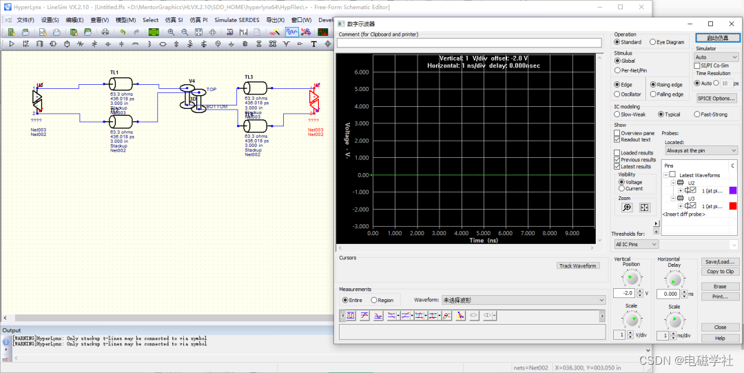
4. HyperLynx LineSim
使用HyperLynx进行建模与ADS有类似之处,不过相比前面介绍的两种,使用HyperLynx显得更加小众一些。分析可能的原因在于,前两者具有更高的与其他软件(仿真格式)进行联仿的兼容性。
- 编辑叠层
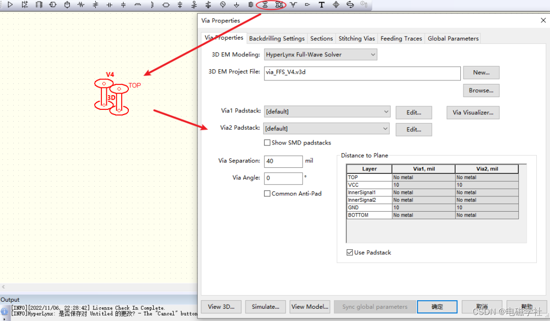
- 编辑过孔
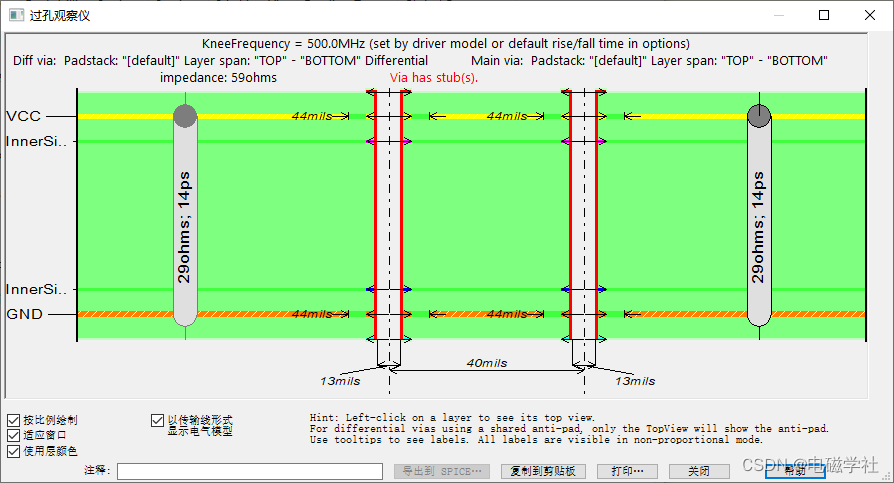
- 过孔截面信息预览
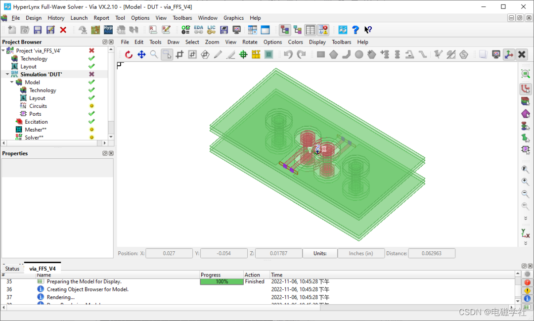
- 3D过孔模型
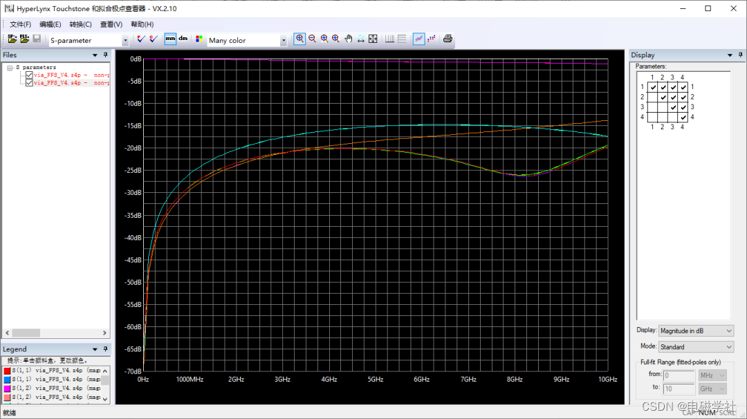
- 仿真得到的过孔S参数
- 在LineSim中进行SI链路级联仿真
关注“电磁学社”,让电磁仿真不再复杂!

电磁学社原创作品 未经授权禁止搬运