1、ERROR:Pack:2530 - The dual data rate register "U_sys_ctl/ODDR2_inst_2" failed to
join an OLOGIC component as required.
错误:
输入时钟50M。PLL出一个228M的clk1和一个148.5M的clk2,clk1对外输出使用,clk2内部信号发生器使用,内部使用的不需要加ODDR2_inst,
解决方案:
去掉ODDR2_inst部分
知识点扩展:.
- 外部管脚输出时,PLL -> BUFG -> ODDR -> PIN,当MAP报错时用 PLL -> BUFG -> ODDR -> OBUFG(IOBUFG) -> PIN
- 内部使用时,PLL -> BUFG->内部使用
2、NgdBuild:770 - IBUFG 'ycbcr28lvds_inst/lvds_tx_1/ibufg_clk_inst' and BUFG 'U_sys_ctl/pll_ip_inst/clkout3_buf' on net 'CLK_297M_OUT' are lined up in series. Buffers of the same direction cannot be placed in series.
错误:
BUFG输出时钟送给了IBUFG,相同方向的缓冲不能串行放置
解决方法:
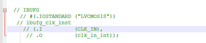
注释掉IP核的IBUFG,
然后在UCF文件中添加约束;
< PIN "U_sys_ctl/pll_ip_inst/clkout1_buf.O" CLOCK_DEDICATED_ROUTE = FALSE; >
知识点扩展:
IBUFG即输入全局缓冲,是与专用全局时钟输入管脚相连接的首级全局缓冲。所有从全局时钟管脚输入的信号必须经过IBUFG单元,否则在布局布线时会报错。 IBUFGDS是IBUFG的差分形式,当信号从一对差分全局时钟管脚输入时,必须使用IBUFGDS作为全局时钟输入缓冲。
BUFG是全局缓冲,它的输入是IBUFG的输出,BUFG的输出到达FPGA内部的IOB、CLB、选择性块RAM的时钟延迟和抖动最小。BUFG连接的是芯片中的专用时钟资源,目的是减少信号的传输延时,提高驱动能力,对于时序电路中的关键时钟信号,这是非常重要的,关系到系统设计的成功与否。如果内部产生的时钟,只在局部模块使用,可以考虑不使用BUFG。一个BUFG只能驱动一个时钟。
3、Place:1318 - User has over-constrained component
ycbcr28lvds_inst/lvds_tx_1/bufio2_inv_inst. There are no placeable sites that
satisfy the user constraints. Please review the user constraints on the
driver component and the load components of
ycbcr28lvds_inst/lvds_tx_1/bufio2_inv_inst.
Phase 4.2 Initial Placement for Architecture Specific Features
解决方法:
BUFPLL needs to have all of its IOB loads placed into the same I/O bank. This error occurs if the user-specified LOC constraints violate this rule.
To resolve the error, make sure all the IOB loads of the BUFPLL instance are locked to the same bank.

可以看出BUFIO2 驱动ODDR2,一个BUFIO2驱动所有的8个ISERDES2,而看原理图可知这8个ISERDES2并不在半个bank上,需要两个BUFIO2去分组驱动不同半BANK上的ISERDES2


所以可以通过创建两个LVDS发送核进行发送,