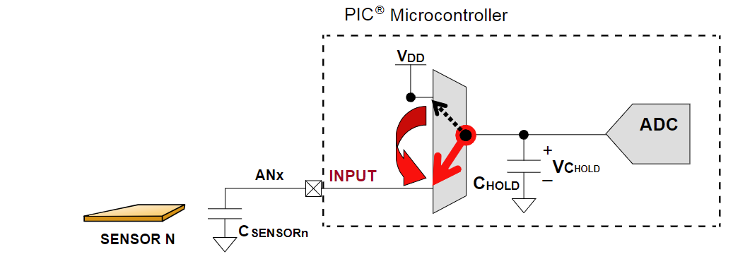
ADC触摸检测原理
ADC内部电容Chold与外部引脚所接电容Csensor并联,等效电容为二者之和。首先将内部电容Chold充电,将外接电容Csensor放电,然后连接二者,将二者电荷量Q保持为恒定值。根据电容公式 Q = CU 可知,当手触摸外部电容Csensor导致其电容增大时,等效电容随之增大,而电荷量Q恒定所以电压U下降。测量得出触摸与未触摸时电压的阈值后就可以根据电压变化来判断是否触摸。
ADC的使用
1、引脚PORT配置
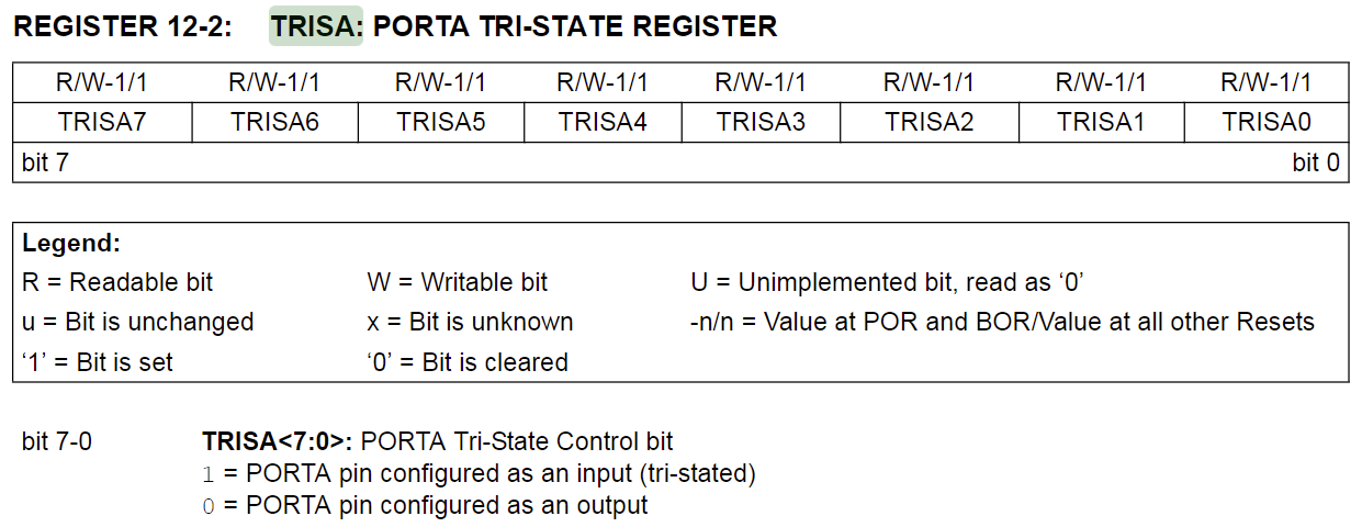
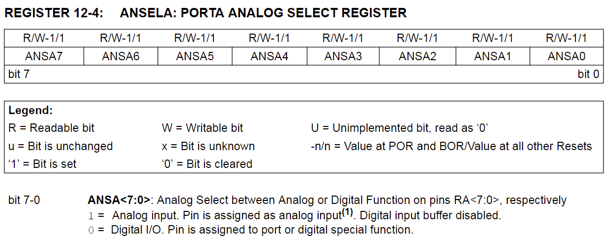
TRISx寄存器控制引脚数据传输方向,ANSELx寄存器控制引脚数据类型为模拟信号还是数字信号。
2、CHANNEL 选择
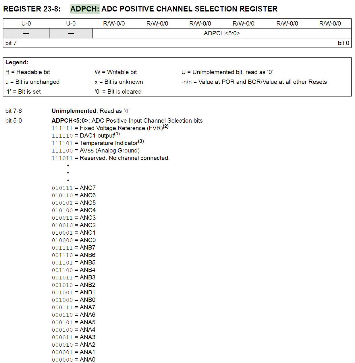
ADPCH寄存器决定channel。
注意,在改变channel后要delay一会儿才能开始下一次转换。
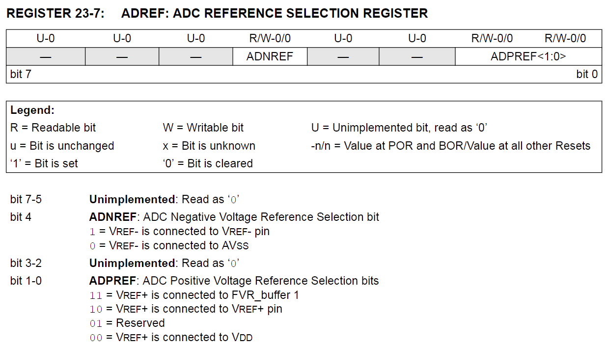
3、选取参考电压
ADREF的ADPREF位选择正参考电压,ADREF的ADNREF位选择负参考电位。
4、CLOCK 选择
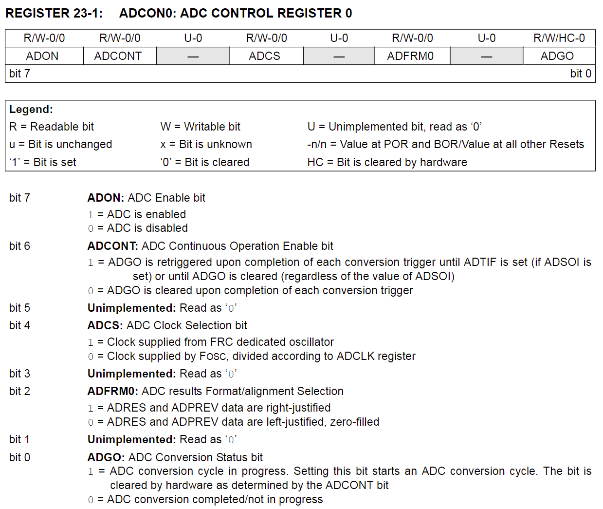
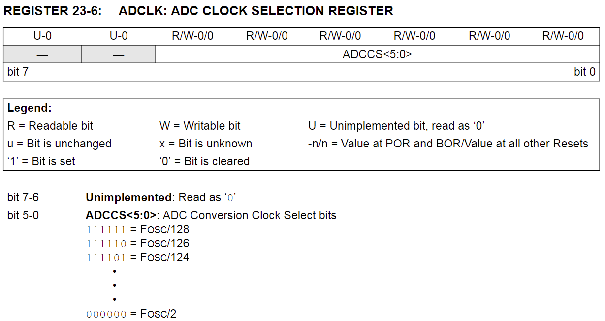
通过ADCON0寄存器的ADCS位和ADCLK寄存器来选择。
5、输出格式控制
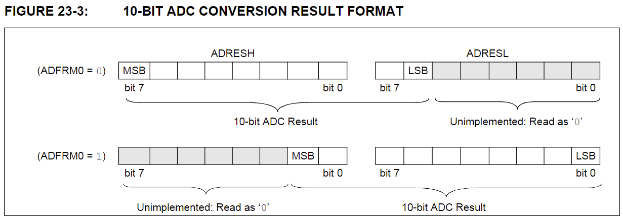
ADC转换结果保存为10bit数据存入ADRES,有两种对齐方式,ADCON0的ADFRM0位决定result的左 / 右对齐。
6、开启ADC
把ADCON0的ADON位置1
7、预充电和采样
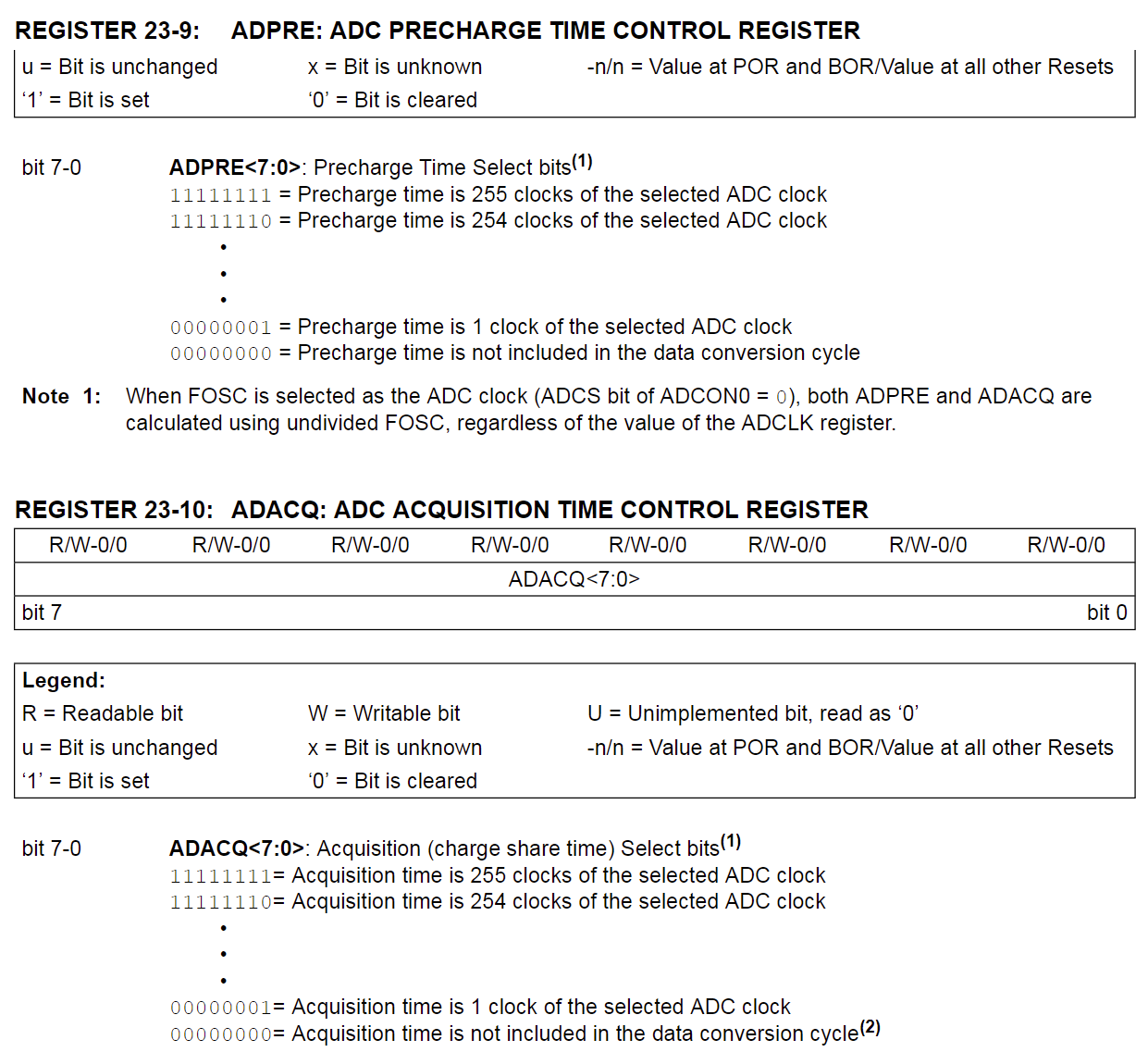
只有外接电容,使用CVD方法实现触摸检测时才进行预充电,作用是对Chold和Csensor充/放电,但是仅仅是进行AD转换则不需要预充电。可通过ADPRE寄存器控制预充电时长。采样是在AD转换之前进行的,时长由ADACQ寄存器设置。必须等待采样结束才能开始AD转换。
8、开启AD转换
把ADCON0的ADGO位置1时开启AD转换,转换结束时ADGO自动清0。应当循环或者定时判断ADGO是否等于0,重复开启AD转换。
9、读取结果
AD转换结果保存在ADRES0L和ADRES0H寄存器,对齐方式在上面已提到。
触摸检测程序设计
实现效果:
按下按键,4位数码管<2:0>显示“YES”,未按下时显示“NO”;数码管<3>显示按下次数,最多记到16次;按下按键时LED灯闪亮。
引脚使用:
PORTA<3:0>为数码管片选位,PORTC<7:0>为数码管段选位;PORTB<7>为LED灯位。
设计思路:
ADC模块循环预充电、采样、AD转换,获取电压变化并与阈值比较判断是否触摸;定时器5ms中断一次,判断ADC是否转换完成,计数并把ADRES中的转换结果同步到数码管的显示缓冲区,随后再次预充电、采样并开启AD转换。
基于PIC16F18854单片机的cC语言源代码:
#include <xc.h>
#ifndef BOOTLOADER//配置段

// PIC16F18854 Configuration Bit Settings

// 'C' source line config statements

// CONFIG1
#pragma config FEXTOSC = OFF   // External Oscillator mode selection bits (Oscillator not enabled)
#pragma config RSTOSC = HFINT1 // Power-up default value for COSC bits (HFINTOSC (1MHz))
#pragma config CLKOUTEN = OFF  // Clock Out Enable bit (CLKOUT function is disabled; i/o or oscillator function on OSC2)
#pragma config CSWEN = ON      // Clock Switch Enable bit (Writing to NOSC and NDIV is allowed)
#pragma config FCMEN = OFF     // Fail-Safe Clock Monitor Enable bit (FSCM timer disabled)

// CONFIG2
#pragma config MCLRE = ON    // Master Clear Enable bit (MCLR pin is Master Clear function)
#pragma config PWRTE = OFF   // Power-up Timer Enable bit (PWRT disabled)
#pragma config LPBOREN = OFF // Low-Power BOR enable bit (ULPBOR disabled)
#pragma config BOREN = ON    // Brown-out reset enable bits (Brown-out Reset Enabled, SBOREN bit is ignored)
#pragma config BORV = LO     // Brown-out Reset Voltage Selection (Brown-out Reset Voltage (VBOR) set to 1.9V on LF, and 2.45V on F Devices)
#pragma config ZCD = OFF     // Zero-cross detect disable (Zero-cross detect circuit is disabled at POR.)
#pragma config PPS1WAY = OFF // Peripheral Pin Select one-way control (The PPSLOCK bit can be set and cleared repeatedly by software)
#pragma config STVREN = ON   // Stack Overflow/Underflow Reset Enable bit (Stack Overflow or Underflow will cause a reset)

// CONFIG3
#pragma config WDTCPS = WDTCPS_31 // WDT Period Select bits (Divider ratio 1:65536; software control of WDTPS)
#pragma config WDTE = SWDTEN      // WDT operating mode (WDT enabled/disabled by SWDTEN bit in WDTCON0)
#pragma config WDTCWS = WDTCWS_7  // WDT Window Select bits (window always open (100%); software control; keyed access not required)
#pragma config WDTCCS = SC        // WDT input clock selector (Software Control)

// CONFIG4
#pragma config WRT = WRT_upper       // UserNVM self-write protection bits (0x0000 to 0x01FF write protected)
#pragma config SCANE = not_available // Scanner Enable bit (Scanner module is not available for use)
#pragma config LVP = ON              // Low Voltage Programming Enable bit (Low Voltage programming enabled. MCLR/Vpp pin function is MCLR.)

// CONFIG5
#pragma config CP = OFF  // UserNVM Program memory code protection bit (Program Memory code protection enabled)
#pragma config CPD = OFF // DataNVM code protection bit (Data EEPROM code protection disabled)

// #pragma config statements should precede project file includes.
// Use project enums instead of #define for ON and OFF.
#endif

unsigned char seq_table[16] = {
    0b00111111, //0
    0b00000110, //1
    0b01011011, //2
    0b01001111, //3
    0b01100110, //4
    0b01101101, //5
    0b01111101, //6
    0b00000111, //7
    0b01111111, //8
    0b01101111, //9
    0b01110111, //a
    0b01111100, //b
    0b00111001, //c
    0b01011110, //d
    0b01111001, //e
    0b01110001  //f
};              //段码表

unsigned char code_table[4] = {
    0b11110111,
    0b11111011,
    0b11111101,
    0b11111110}; //位码表

unsigned char display_table[4]; //显示缓冲区
int touch_count;                //按动次数计时器
int touch_flag;                 //按动记录标志位
int mode = 0;                   //mode == 0 means print "yes" or "no"; mode == 1 means print voltage ADC number

void __interrupt() ISR(void);
void seq_code_sel(int i);
void Init();
void Init_timer();
void Init_ADC();

void main(void)
{
    unsigned char i = 0;
    touch_count = 0;
    touch_flag = 0;

    Init();

    while (1)
    {
        seq_code_sel(i);
        i = (i + 1) % 4;
    }
}

void __interrupt() ISR(void)
{
    PIR0bits.TMR0IF = 0; //clear the signal bit
    TMR0H = 0x3c;
    TMR0L = 0xb0;

    if (mode)
    {
        if (ADRES)
        {
            display_table[0] = touch_count;
            display_table[1] = (ADRES / 100) % 10;
            display_table[2] = (ADRES / 10) % 10;
            display_table[3] = ADRES % 10;
        }
    }
    else
    {
        if (ADRES > 800) //设置阈值为 800
        {
            PORTB = 0;

            display_table[0] = seq_table[touch_count];
            display_table[1] = 0;
            display_table[2] = 0x37;
            display_table[3] = 0x3f;
            touch_flag = 1;
        }
        if (ADRES < 800)
        {
            PORTB = 0x80;

            if (touch_flag)
            {
                touch_count = (touch_count + 1) % 16;
                touch_flag = 0;
            }
            display_table[0] = seq_table[touch_count];
            display_table[1] = 0x6e;
            display_table[2] = 0x7b;
            display_table[3] = 0x6d;
        }
    }

    if (ADCON0bits.ADGO == 0)
    {
        ADPRE = 0b00010000; //Precharge time is 128 clocks of the selected ADC clock
        ADACQ = 0b00010000; //Acquisition time is 128 clocks of the selected ADC clock
        for (int wait = 0; wait < 16; wait++); //wait for acquisition time
        ADCON0bits.ADGO = 1;
    }
}

void Init()
{
    //Init PORTA,PORTB,PORTC
    PORTA = 0;
    LATA = 0;
    ANSELA = 0x80;
    TRISA = 0x80; //Set RA7 to input

    PORTB = 0;
    LATB = 0;
    ANSELB = 0;
    TRISB = 0;

    PORTC = 0;
    LATC = 0;
    ANSELC = 0;
    TRISC = 0;

    Init_timer();
    Init_ADC();
}

void Init_ADC()
{
    //Init ADC
    ADCLKbits.ADCCS = 0b000001; //FOSC/4

    ADCON1bits.ADPPOL = 0; //IO pin shorted to VSS, Chold shorted to AVDD
    ADCON0bits.ADCS = 0;   //Clock supplied by FOSC, divided according to ADCLK register
    ADCON0bits.ADFRM0 = 1; //ADRES and ADPREV data are right-justified

    ADREFbits.ADPREF = 0b11; //VREF+ is connected to FVR
    ADREFbits.ADNREF = 0b0;  // VREF- is connected to VSS

    FVRCONbits.FVREN = 1;    //FVR enable
    FVRCONbits.ADFVR = 0b11; //ADC FVR Buffer Gain is 4x, (4.096V)
    FVRCONbits.FVRRDY = 1;   //Fixed Voltage Reference output is ready for use

    ADCON1 = 0b00000000; // default ADPPOL, no ADDSEN
    ADCON2 = 0b00000000; // legacy mode
    ADCON3 = 0b00000000; // default, no interrupt

    ADPCH = 0b000111;   //ADC Positive Input Channel Selection == RA7
    ADCAP = 0b101;      //ADC Additional Sample Capacitor == 5pF
    ADPRE = 0b00010000; //Precharge time is 128 clocks of the selected ADC clock
    ADACQ = 0b00010000; //Acquisition time is 128 clocks of the selected ADC clock
    for (int wait = 0; wait < 16; wait++);//wait for acquisition time
    ADCON0bits.ADON = 1; //Turn ADC On
}

void Init_timer()
{
    //Timer interrupt
    INTCONbits.GIE = 1;
    PIR0bits.TMR0IF = 0; //clear the signal bit
    PIE0bits.TMR0IE = 1; //interrupt enable

    //Timer0 configuration
    T0CON0 = 0b00010000;
    T0CON1 = 0b01000000;
    TMR0H = 0x3c;
    TMR0L = 0xb0;
    T0CON0bits.T0EN = 1;
}

void seq_code_sel(int i)
{
    PORTA = code_table[i];
    if (mode)
    {
        PORTC = seq_table[display_table[i]];
    }
    else
    {
        PORTC = display_table[i];
    }

    for (int temp = 0; temp < 100; temp++);
}