牛客上组合逻辑部分的题也刷完了,详见主页的FPGA刷题P3和P4,接下来把最后一部分刷了

也就是时序逻辑部分:

目录
根据状态转移表实现时序电路
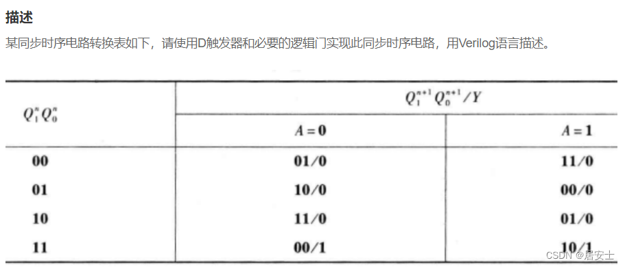
首先要看懂这个表,第一列是现态,A是跳转条件,A下面的 跳转的状态/输出的结果
接下来我们把状态转移表变成状态转移图:
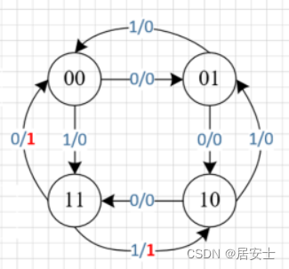
根据状态转移图写代码:
module seq_circuit(
      input                A   ,
      input                clk ,
      input                rst_n,

      output   wire        Y
);
    parameter s0=2'b00    ;
parameter s1=2'b01    ;
parameter s2=2'b10    ;
parameter s3=2'b11    ;

reg  [1:0]cur_state   ;
reg  [1:0]next_state  ;
reg  Y0               ;

// one step
always@(posedge clk or negedge rst_n)begin
    if(!rst_n)
        cur_state<=s0           ;
    else
        cur_state<=next_state   ;
end

// tow step
always@(*)begin
    case(cur_state)
        s0: next_state = A ? s3 : s1    ;
        s1: next_state = A ? s0 : s2    ;
        s2: next_state = A ? s1 : s3    ;
        s3: next_state = A ? s2 : s0    ;
        default: next_state = s0        ;
    endcase
end

 always @(*) begin
    if(!rst_n)
        Y0 <= 1'b0                ;
    else begin
        case(cur_state)
            s0 : Y0 = 1'b0        ;
            s1 : Y0 = 1'b0        ;
            s2 : Y0 = 1'b0        ;
            s3 : Y0 = 1'b1        ;
            default : Y0 = 1'b0   ;
        endcase
    end
end

assign Y = Y0  ;

endmodule
根据状态转移图实现时序电路
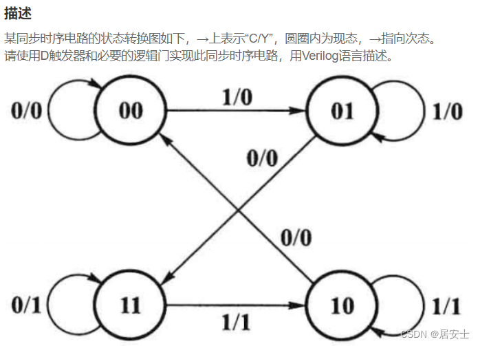
这一题直接给出了时序电路图,我们用Verilog语言描述:
module seq_circuit(
   input                C   ,
   input                clk ,
   input                rst_n,

   output   wire        Y
);
    reg y;
    reg [1:0] current_state,next_state;

    always@(posedge clk or negedge rst_n )begin
        if(~rst_n)begin
            current_state<=2'b00;
        end
        else begin
            current_state<=next_state;
        end
    end

    always@(*)begin
        case(current_state)
            2'b00:next_state=C?2'b01:2'b00;
            2'b01:next_state=C?2'b01:2'b11;
            2'b10:next_state=C?2'b10:2'b00;
            2'b11:next_state=C?2'b10:2'b11;
        endcase
    end

    always@(*)begin
        if(~rst_n)begin
            y=1'b0;
        end
        else begin
           case(current_state)
            2'b00:y=1'd0;
            2'b01:y=1'd0;
            2'b10:begin
                if(C==1'd0)begin
                    y=1'd0;
                end
                else begin
                    y=1'd1;
                end
            end
            2'b11:y=1'd1;
        endcase
        end
    end

    assign Y=y;

endmodule
ROM的简单实现
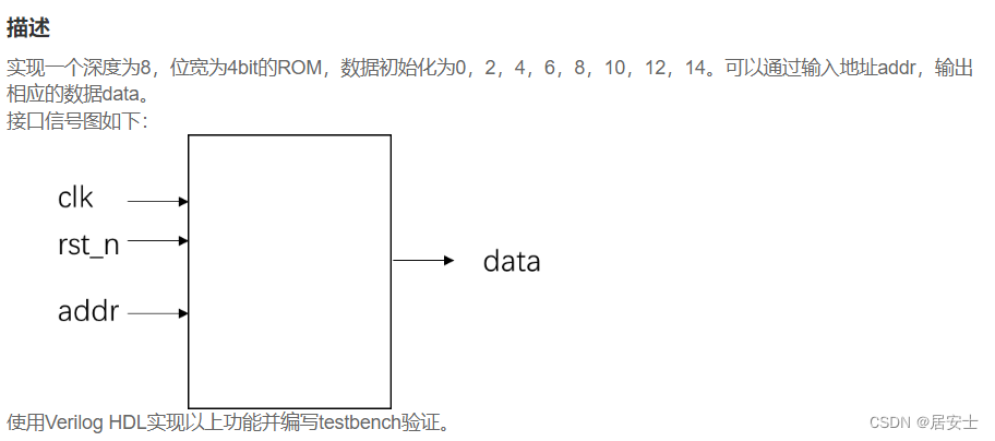
这个题要把地址和数据对应起来,ROM初始化的时候存入,后面只能读,深度为8恰好存满了
对于二维数组 定义方式:reg 【位宽】参数 【深度】;
module rom(
	input clk,
	input rst_n,
	input [7:0]addr,

	output [3:0]data
);

    reg [3:0] rom[7:0];//前面是位宽,后面是深度
    integer i;

    always@(posedge clk or negedge rst_n )begin
        if(~rst_n)begin//初始化
           rom[0] <= 4'd0  ;
           rom[1] <= 4'd2  ;
           rom[2] <= 4'd4  ;
           rom[3] <= 4'd6  ;
           rom[4] <= 4'd8  ;
           rom[5] <= 4'd10 ;
           rom[6] <= 4'd12 ;
           rom[7] <= 4'd14 ;
        end
        else begin
            for(i=0;i<8;i=i+1)begin: rom_i //保持数据
                rom[i]<=rom[i];
            end
        end
    end

    assign data=rom[addr];

endmodule
边沿检测

这个题是叫我们产生上升沿和下降沿的信号
首先打一拍产生一个dly信号
上升沿:原始信号=1 && dly信号=0
下降沿:原始信号=0 && dly信号=1
module edge_detect(
	input clk,
	input rst_n,
	input a,

	output reg rise,
	output reg down
);
reg a_dly;
    always@(posedge clk or negedge rst_n)begin
    if(~rst_n) begin
         rise<=0;
         down<=0;
    end
    else begin
        a_dly <= a;
        if ((~a_dly)&a)
            rise <= 1;
        else
            rise <= 0;

        if ((~a)&a_dly)
            down <= 1;
        else
            down <= 0;
    end

end
endmodule
综上,牛客上Verilog部分的基础刷题都完成了!