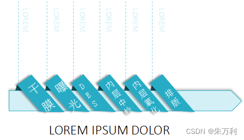
PCB production process three: What are the 7 steps to produce the inner layer circuit of PCB
The first step in our PCB production process is the inner layer circuit, so what are the steps in its process? Next, we will take the flow of the inner line as the theme and conduct a detailed analysis.

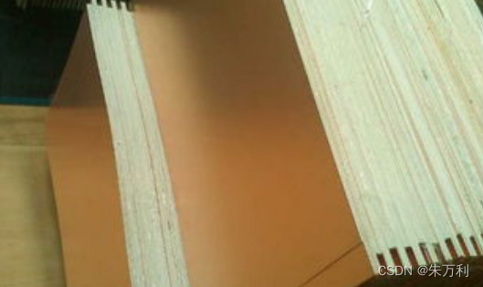
It is made of prepreg and copper foil, and is used as a raw material for PCB production, also known as copper clad laminate.
The general specifications are:
Dimensions:
"37 49", "41 49", etc.
Thickness specification:
2mil, 4.5mil, 6mil, 7.5mil, 8mil, etc.
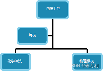
1. Cutting material:
Cut a large sheet of material into the required production size according to the size requirements of different versions.
2. Baking material:
In order to eliminate the internal stress generated during the production of the sheet and to strengthen the dimensional stability of the sheet. Remove moisture absorbed by the sheet during storage, enhancing the reliability of the material.
3. Gong fillets:
In order to avoid handling and quality problems in the next process, the sheet is rounded.
1. Degreasing: Remove the oxide film of oily substances on the copper surface by acidic chemicals.
2. Micro-etching: The principle is that oxidation-reduction reactions occur on the copper surface to roughen the copper surface.
3. Pickling: remove copper ions and reduce oxidation of copper surface
4. Drying with hot air: Dry the surface of the board.
1. Development:
Under the action of the potion sodium carbonate, the ink of the unexposed part is dissolved and rinsed, and the photosensitive part is thrown away.
2. Etching:
The copper surface of the unexposed exposed copper part is etched away.
3. Withdrawing the film:
The ink protecting the copper surface of the circuit is removed by a higher concentration of sodium hydroxide.
4. Punching:
Through the set target, punch out the tube position hole at the uniform position of each layer, and use it for positioning in the next process.
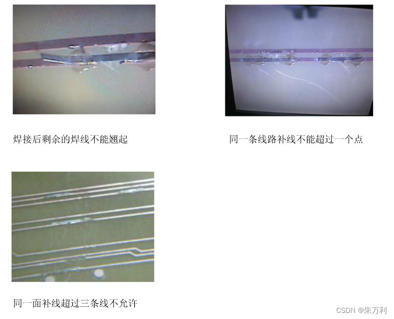
1. Optical inspection:
It is a device based on optical principles to detect common defects encountered in welding production. AOI is a new type of testing technology emerging, but it is developing rapidly, and many manufacturers have launched AOI testing equipment. During automatic detection, the machine automatically scans the PCB through the camera, collects images, compares the tested solder joints with the qualified parameters in the database, and after image processing, checks out the defects on the PCB, and displays/marks the defects through the display or automatic signs out for repair by the maintenance crew.
2. Target check confirmation:
Confirm by visual inspection, and confirm or eliminate some true and false defects.
3. Visual inspection and sub-board:
Repair or scrap confirmed defects, and classify different layers.