LED light flashing routine explanation

Based on many years of work experience, the FPGA design process has been summarized in a total of the above 12 steps, some of which can be omitted depending on the difficulty of the project. For example, for very simple projects, we can omit the steps in the dotted box, but our introductory course, no matter how simple it is, will be explained according to these 12 steps.
1. Interpretation of requirements
1.1 Requirements
Realize that the LED light (D2) flashes once every 1 second
1.2 Knowledge background
Introduction to LED lights
LED, also known as light-emitting diodes. The operating current of LED lights is very small (some can emit light with only a few tenths of a milliamp). They have good impact and seismic resistance, high reliability and long life. Due to these advantages, LED lights are widely used in instruments and meters as indicator lights, LCD screen backlights and many other fields. Light-emitting diodes of different materials can emit eight colors of light: red, orange, yellow, green, cyan, blue, purple and white. As shown below:


1.3 Hardware design


The schematic diagram of the light-emitting diode is shown in Figure 4 above. The anodes of the eight light-emitting diodes from LED1 to LED8 are connected to 3.3V, and the cathodes are connected to the corresponding pins of the FPGA. The resistor between the LED and ground in the schematic diagram acts as a current limiter. We can see from the schematic diagram that LED1 is connected to pin L12 of FPGA. We have marked the pin numbers on the PCB diagram or the actual object, so when binding the pins, you don’t need to look at the schematic diagram, just look at the silk screen on the board, as shown in the PCB diagram above. We only light one LED light (LED1), then we only need to care about the pin number (L12) of LED1. When pin L12 outputs a low level, current flows through the LED light, driving the LED light to emit light. If L12 outputs a high level, no current flows through the LED light, and the LED does not emit light.
1.4 Interface description
| Signal name | direction | FPGA pin number | illustrate |
|---|---|---|---|
| LED0 | output | L12 | Connected to LED light, low level LED light turns on |
| CLK50M | enter | B10 | Clock signal, 50MHZ |
| KEY1 | enter | E4 | Independent button, press low level, used as reset |
Summary: Through the above explanation, the requirement can be interpreted as, as long as the L12 pin of the FPGA is set to low level (500ms), the LED light D2 can be lit for 500ms, and then the L12 pin is set to high level ( 500ms), that is, the LED light D2 can be turned off for 500ms. In this cycle, the effect of flashing once per second is achieved.
2. Draw theoretical waveform diagram
clk is a 50Mhz clock, one cycle is 20ns, 1 second = 1000000000ns, 1 second is 50000000 clock cycles, 500ms = 25000000 clock cycles.

3. New TD project
In order to make the project look tidy and facilitate project transplantation. We create 4 new folders, namely Project, Source, Sim, and Doc.
Project — the project folder, which contains the TD project
Source — the source code folder, which contains the project source code (.v file or .vhd file)
Sim — the simulation folder, which contains the simulation-related files
Doc — stores relevant information , such as data manuals, requirements documents, etc.
4. Write code
 ///
//QQ:3181961725
//TEL/WX:13540738439
//作者:Mr Wang
//模块介绍:实现LED灯(D8)间隔1秒闪烁1次
///
module led_ctrl(
	input		clk		,//时钟,50MHZ
	input		rst_n	,//复位,低电平有效
	output	reg	led		 //LED灯控制信号
	);
	parameter	time_500m=25000000;//500ms
	//为了缩短仿真时间,减小了参数值,仅仅用于仿真
	//parameter	time_500m=2500;//500ms
	reg	[24:0] cnt;
	always@(posedge clk or negedge rst_n)begin
		if(!rst_n)
			cnt<=0;
		else if(cnt==time_500m-1)
			cnt<=0;
		else
			cnt<=cnt+1;
	end
	always@(posedge clk or negedge rst_n)begin
		if(!rst_n)
			led<=1;
		else if(cnt==time_500m-1)
			led<=~led;
		else;
	end
endmodule
5. Write simulation test stimulus file

 ///
//QQ:3181961725
//TEL/WX:13540738439
//作者:Mr Wang
`timescale 1ns/1ns
module led_ctrl_tb;
	reg	clk;
	reg	rst_n;
	initial
		begin
			clk=0;
			rst_n=0;//生成复位激励信号
			#1000
			rst_n=1;//生成复位激励信号
		end
	//生成时钟激励信号
	always #10 clk<=~clk;
	//例化被仿真模块
	led_ctrl Uled_ctrl(
	.clk		(clk	),
	.rst_n		(rst_n	),
	.led        (		)
	);
endmodule
During simulation, our main concern is the input port. In the led_ctrl module, there are two input ports, rst_n, clk. Therefore, when we write the simulation test file, we pour excitation signals into these two ports.
6.Modelsim simulation
This routine is very simple and uses only one statement, so no simulation verification is required. But in order to demonstrate a complete development process to everyone, we also created a new simulation project for this experiment, starting from the simplest code to teach you how to write simulation stimulus files and how to use Modelsim software for simulation. Add the source code written in the third step and the simulation test stimulus file written in the fourth step to the Modelsim simulation project to simulate and observe the waveform.
There are generally two methods for Modelsim simulation:
-
Graphical interface simulation means that all operations are completed on the Modelsim software interface. The advantage of this method is that it is easy to learn and suitable for simple projects. The disadvantage is that the operation steps are cumbersome.
-
Batch simulation , this method requires writing corresponding script files before simulation. The advantage of this method is that the simulation can be completed with one click, saving time and effort. The disadvantage is that script files need to be written in the early stage. In order to quickly apply what everyone has learned to engineering practice, only the first experiment and the second experiment were simulated using a graphical interface, and all subsequent experiments were simulated using batch processing.
Graphical interface simulation steps:
1. Create a new project, file–>new–>Project

2.填写工程名以及指定仿真工程存放路径

3. Add files, source files and simulation stimulus files
4. Compile
5. Start simulation


6. Add observation signal

7. Interrupt simulation

8. Enter the run command, run + simulation time

At this point, we can observe the level status of the simulated signal in the waveform window.
When we change the source code, we need to start from step 4 again.
The simulated waveform is shown in the figure below:

7. Compare waveforms
Compare the theoretical waveform diagram drawn in the second step with the waveform diagram simulated by Modelsim in the sixth step. The results are consistent, indicating that our logic design is correct. If the comparison results are found to be inconsistent, you need to find the reason for the inconsistency, and ultimately ensure that the comparison results are consistent.
By comparison, the theoretical waveform is consistent with the simulated waveform, indicating that the function meets the design requirements.
8 Add .v file

9 Bind the pins and save the constraint file (.adc)


10 Compile and synthesize the BIT file

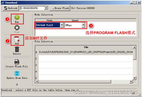
11. Download BIT file


After the download is successful, you can observe the experimental phenomena on the development board. If the experimental phenomena match the design requirements, it means that there is no problem with our design, and we can proceed to the next step of solidifying the configuration file.
12 solidification configuration file
FPGA has a characteristic that the configuration information will be lost after power failure, so we need to store the configuration information in the configuration chip (FLASH). After the development board is powered on, the FPGA will read the configuration information in the configuration chip, so the development The board can still work normally after powering off and on again.
After the curing is successful, power off the development board and then power it on again. It can be observed that the development board can still perform the functions just now.
Experimental phenomena
The LED light connected to FPGA pin L12 achieves the effect of flashing once per second, which meets the design requirements and the design is completed!