This article quotes TI documents
pressure drop
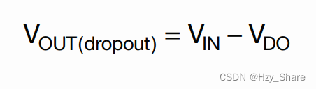
The dropout voltage VDO refers to the minimum voltage difference at which the input voltage VIN must be higher than the required output voltage VOUT(nom) to achieve normal voltage regulation.

If VIN falls below this value, the linear regulator operates in dropout and no longer regulates the desired output voltage. In this case, the output voltage VOUT(dropout) will be equal to VIN minus the dropout voltage.
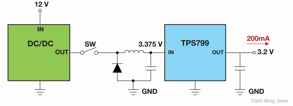
Take an LDO such as the TPS799 with a regulated voltage of 3.3V as an example: When outputting a current of 200mA, the maximum dropout voltage of the TPS799 is specified as 175mV. As long as the input voltage is 3.475V or higher, it will not affect the regulation process. However, dropping the input voltage to 3.375V will cause the LDO to operate in a dropout condition and stop regulating.
Factors that determine pressure drop
The voltage drop is mainly determined by the LDO architecture.
To illustrate why, let's take a look at P-channel metal-oxide semiconductor (PMOS) and N-channel MOS (NMOS) LDOs and compare their operation.
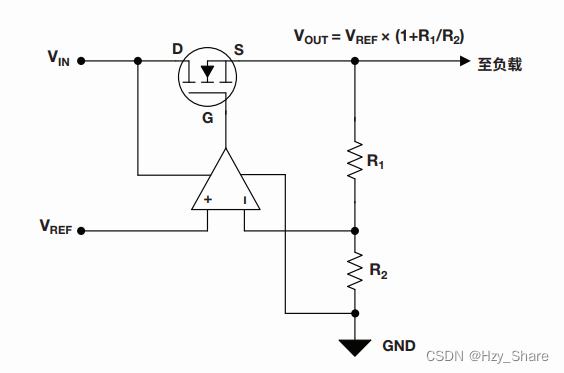
PMOS LDO
PMOS LDO architecture shown. To regulate the desired output voltage, the feedback loop controls the drain-source resistance RDS. As VIN gradually approaches VOUT(nom), the error amplifier will drive the gate-source voltage VGS to increase negatively to reduce RDS and maintain regulation.
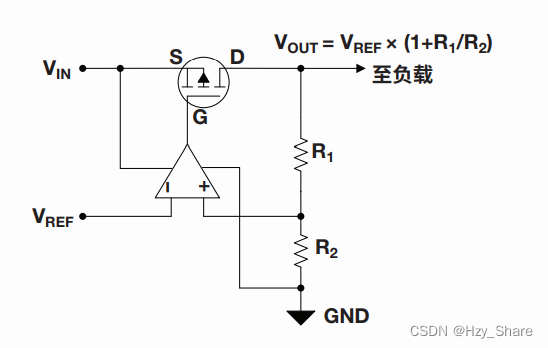
However, at a certain point, the error amplifier output will saturate at ground and will be unable to drive VGS further negative. RDS has reached its minimum value. Multiplying this RDS value by the output current IOUT will give you the dropout voltage.
As VGS increases in the negative direction, the lower RDS value that can be achieved. By increasing the input voltage, the VGS value can be increased in the negative direction. Therefore, PMOS architecture has lower voltage drop at higher output voltages.
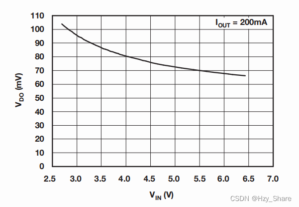
As shown in the figure, the dropout voltage of the TPS799 decreases as the input voltage (which also applies to the output voltage) increases. This is because VGS increases negatively as the input voltage increases.
NMOS LDO
The NMOS architecture is shown in the figure, and the feedback loop still controls the RDS. However, as VIN approaches VOUT(nom), the error amplifier will increase VGS to reduce RDS, thus maintaining regulation.
At a certain point, VGS cannot rise any higher because the error amplifier output will saturate at the supply voltage, VIN. When this state is reached, RDS is at its minimum value. Multiplying this value by the output current IOUT yields the dropout voltage.
Biased LDO
Many NMOS LDOs use an auxiliary voltage rail, the bias voltage VBIAS
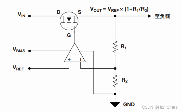
This voltage rail serves as the positive supply rail for the error amplifier and allows its output to swing all the way to VBIAS above VIN. This configuration allows the LDO to maintain a high VGS, resulting in ultra-low dropout at low output voltages.
Sometimes an auxiliary voltage rail is not provided, but low dropout at a lower output voltage is still required. In this case, VBIAS can be replaced by an internal charge pump
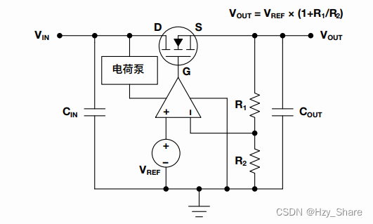
The charge pump will boost VIN so that the error amplifier can still generate a larger VGS value in the absence of the external VBIAS voltage rail.
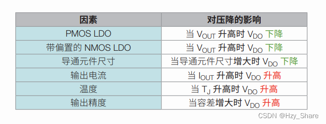
In addition to architecture, voltage drop can be affected by several other factors
Original text: https://www.ti.com.cn/cn/lit/eb/zhcy089a/zhcy089a.pdf