前言
项目用到MiniPCIe标准接口,这里介绍硬件接口、结构尺寸、以及对应封装。
miniPCIe封装下载链接
一、标准规范
标准参考《Mini PCI Express™ Card Electromechanical Specification Revision 1.0》。
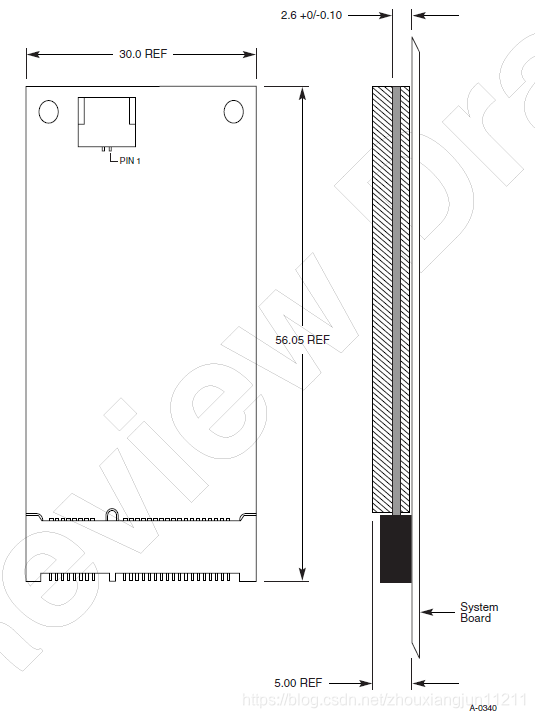
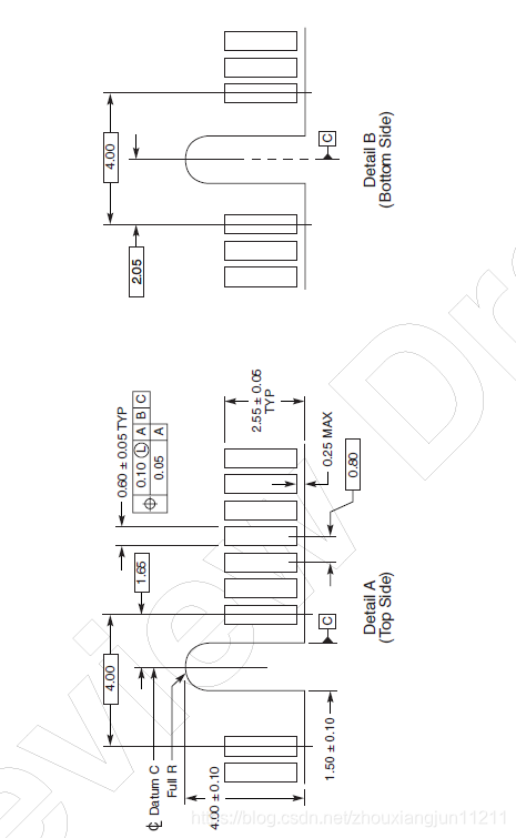
二、板卡外形
板卡外形尺寸
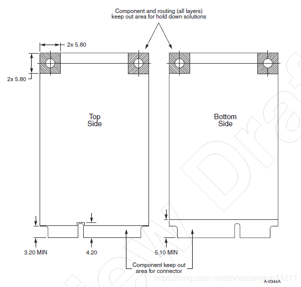
1. 结构细节
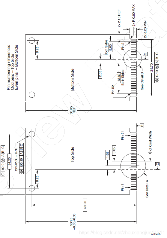
2. 板卡禁布区间
3. PCB封装图
Altium Designer封装

miniPCIe封装下载链接:https://download.csdn.net/download/zhouxiangjun11211/13631384
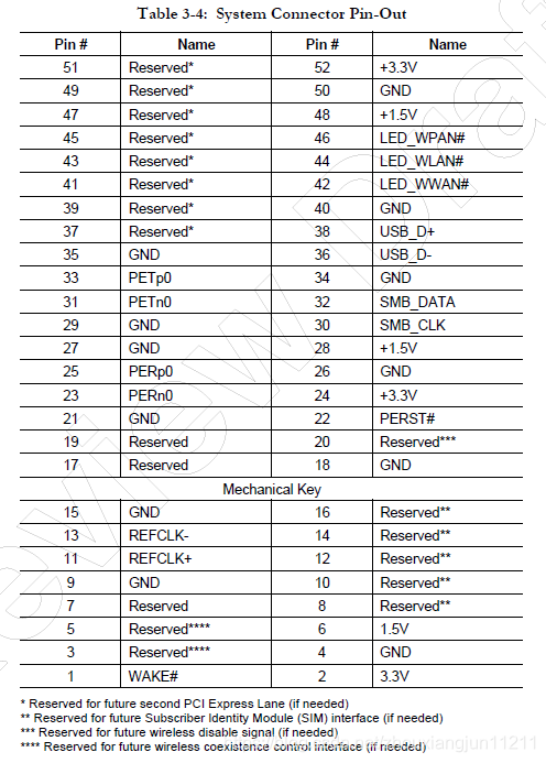
三、接口定义
miniPCIe 接口
| Signal Group | Signal | Direction | Description |
|---|---|---|---|
| Power | +3.3V(3 pins) | Primary 3.3V source | |
| Power | +1.5V(3 pins) | Primary 1.5V source | |
| Power | GND(12 pins) | Return current path | |
| PCI Express | PETp0,PETn0,PERp0,PERn0 | Input/Output | PCI Express × 1 \times1 ×1data interface:one differential transmit pair and one differential receive pair |
| PCI Express | REFCLK+,REFCLK- | Input | PCI Express differential reference clock(100MHz) |
| USB | USB_D+,USB_D- | Input/output | USB serial data interface compliant to USB 2.0 specification |
| Auxiliary Signals (3.3V Compliant) | PERST# | Input | Functonal reset to the card |
| Auxiliary Signals (3.3V Compliant) | WAKE# | Output | Open Drain active Low signal |
| Auxiliary Signals (3.3V Compliant) | SMB_DATA | Input/Output | SMBus data signal compliant to the SMBUS 2.0 specification |
| Auxiliary Signals (3.3V Compliant) | SMB_DATA | Input | SMBus data signal compliant to the SMBUS 2.0 specification |
| Communications Specific Signals | LED_WPAN#,LED_WLAN#,LED_WWAN# | Output | These signals are used to allow the Mini PCI Express add-in card to provide status indicators via LED devices that will be provided by the system |