In the previous lab(Memory-mapped I/O), we have used both the PS and PL sides of the Zynq chip. A software was running on the ARM processor to implement a binary counter. The same counter’s specifications will be implemented in this lab but using a completely different method. In this lab, we will only use the PL-side of the chip. the exact same functionality is implemented by hardware circuits only. The functionality of the hardware is described using Verilog HDL (Hardware Description Language), the Verilog synthesizer will convert the Verilog file into circuit’s netlists. This lab will give you a good start up guide on hardware design flow, which involves among many steps: specification, design, simulation, and verification.
Lab2 Design Flow
Lab2 Block Diagram
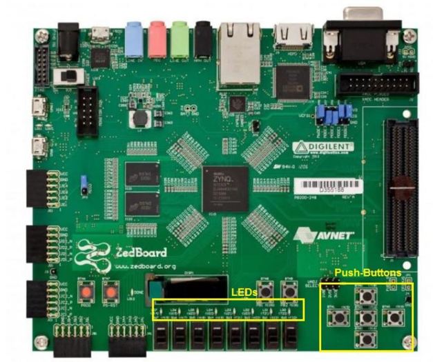
Lab2 Board Interface
The design methodology followed in this lab is a simplified one of what would a hardware engineer typically follow to implement a hardware circuit or an IP. The IP blocks we have easily used in the previous lab have been implemented in a similar fashion, they also have Verilog HDL(or other HDL) files written by developers and wrapped up as a user friendly plug and play IP. The Verilog source code for Lab2 is available Here. You will simulate the Verilog design to test functionality and to catch any errors in Verilog files, after doing so, you will implement the design , generate a Bitstream , download it to Zedboard and verify functionality in hardware. You will notice identical behavior of Lab1. This will give you an insight that the same functionality implemented in software could be implemented in hardware(Its relatively more complicated to implement functionality in hardware,however, sometimes it can lead to substantial performance improvements) .
Objectives
1.Use Vivado to create a simple hardware HDL design targeting the ZedBoard.
2.Examine the Vivado project directory structure, and get familiarized with the directories created by Vivado to store imported source code, new code, reports and outputs.
3.Perform RTL analysis on the design, analyze the different schematics generated by Vivado for the HDL design.
4.Perform hardware utilization measurements for the design in both post-synthesis (estimation) and post-implementation. Hardware utilization provides the percentage of how much hardware resources are used within the chip.
5.Introduce Vivado Simulator, perform behavioral simulation, write Verilog testbenches, and analyzing waveforms.
Procedures

A-Download Source Code from GitHub
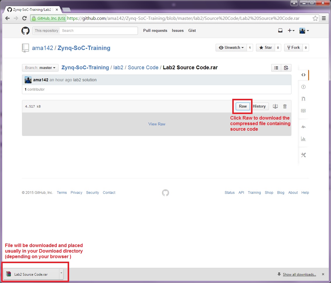
Download Lab2 Verilog source files and constraints file from My GitHub Page here. To download a file in GitHub, Click on file name first( In this case its a compressed file named Lab2 Source Code) . Then on the next page that opens, click Raw to download the file.
GitHub Zynq SoC Training Source Code Repository
Download Source Code from GitHub
Make sure to extract the compressed file in a directory that you can easily refer to. After extraction, you will find four Verilog files and one constraint file.
Source code after extracting from the compressed file
B-Create a project in Vivado to target the Zedboard
1.Launch Vivado Design Suite.
2.Click on File-> New project, to open the New Project wizard.
New Project Wizard
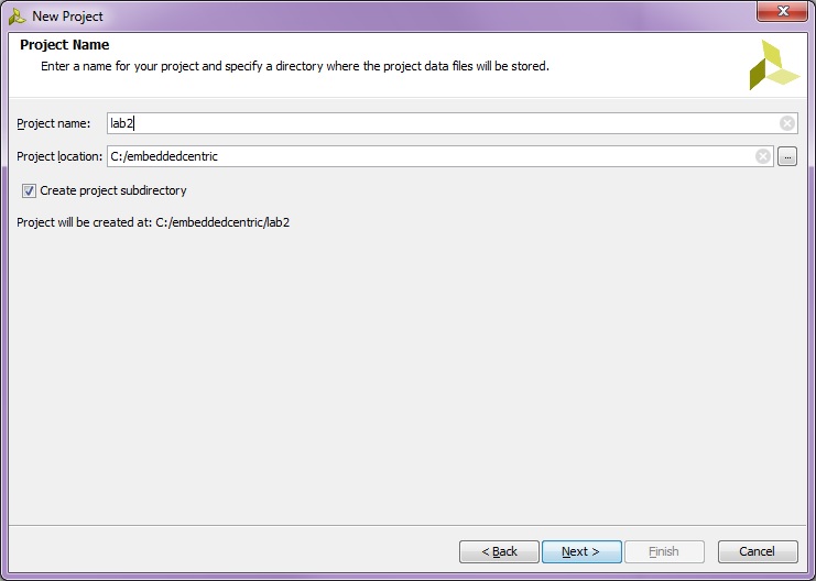
3.In the next window enter “lab2” as the Project name. Specify the directory in which to store the project files ”C:/embeddedcentric”- leave the Create Project Subdirectorychecked.
Project Name and Location
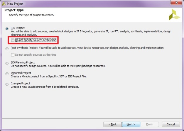
4.Next, specify the project type. Use the default selection, RTL Project. Make sure Do not specify sources at this time is unchecked. As we will import source code and constraint file to Vivado.
Project Type (Uncheck Do not specify sources at this time)
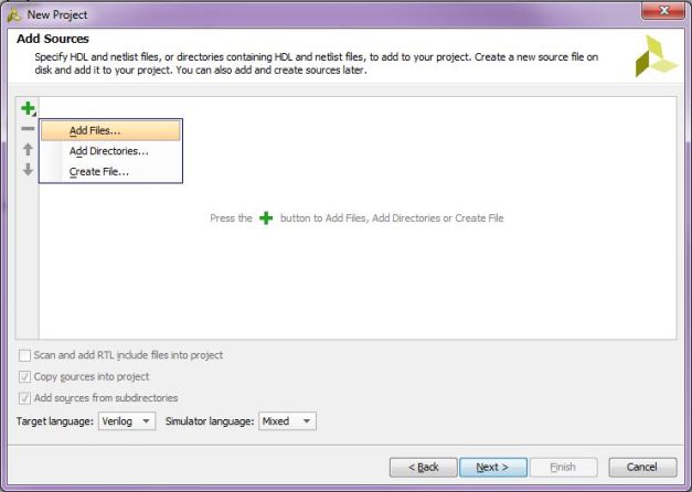
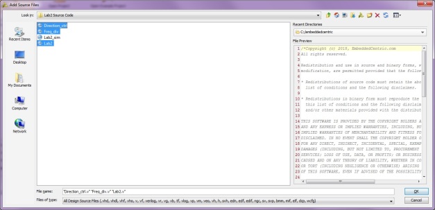
5.In the Add Sources window, click on the green + symbol and select Add Files. Refer to the directory where you extracted the source code and select the following three files by holding the Ctrl key(Lab2.v,Freq_div.v,Direction_ctrl.v). These files represent the hardware design files for Lab2. Click OK. Make sure that Copy Sources into projectis checked in the Add Sources window. Click Next twice to skip the Add Existing IP window( No IP will be added in this design) .
Add Sources
Add the design files for lab2
Add Sources window after adding files
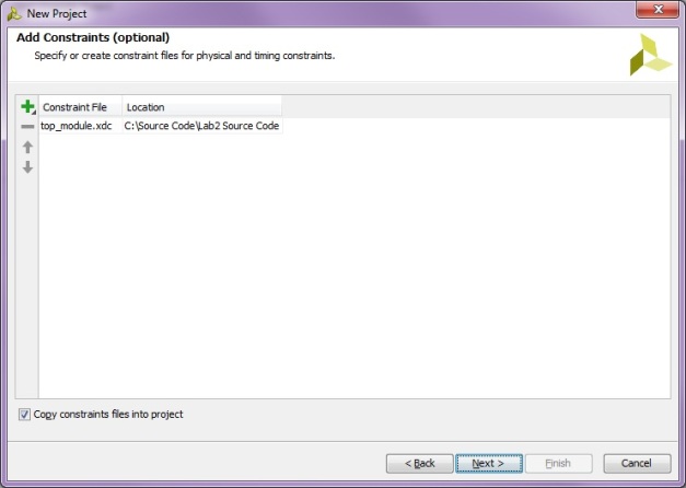
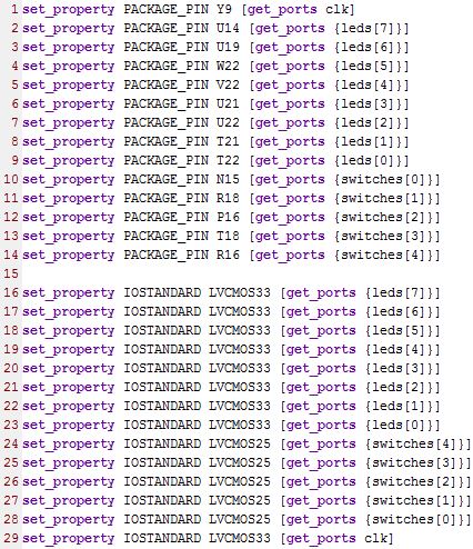
6.In the Add Constraints window , Click the green + symbol and select Add Files,Refer to the directory where you extracted the source code and select file top_module.xdc, make sure Copy constraints files into project is checked, click Next. This file contains physical constraints for the LEDs, push buttons and also a clock . these constraints links ports defined in the Verilog files to actual pins on Zedboard.
Add Constraints Window
Constraint File top_module.xdc
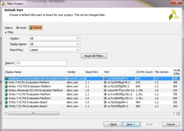
7.Next, specify the board that you want to test your project on. Zedboard.Click Nextthen click Finish.
Default Part
C-Explore the Vivado’s project directory structure
This section will show you how Vivado organizes source codes in separate directories. Use the Windows Explorer and view directory “C:\embeddedcentric\lab2” . You will find lab2.cache, lab2.hw,lab2.sim, lab2.srcs directories and lab2.xpr Vivado project file have been created. The lab2.cache directory is a place holder for the Vivado program database. Inside lab2.srcs, two directories exists constrs_1 and sources_1, ; inside these directories , the copied top_module.xdc (constraints) and Lab2.v , Freq_div.v , Direction_ctrl.v (source code) files respectively are stored.( We will cover the other directories in later sections)
Vivado Project Directory Structure
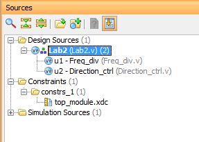
Go back to Vivado, in the Sources pane, double click on Lab2. Notice that the Freq_div and Direction_ctrl are in a lower hierarchical level than Lab2. This is because Lab2 is the top level model of the Verilog design and it is instantiating both Freq_div and Direction_ctrl as Verilog instances. Also pay attention that the top_module.xdc constraints file we imported previously is located in the Constraints tab under constrs_1.
Vivado Sources Pane
D-Perform RTL analysis on the source file
Register Transfer Level (RTL) analysis can provide you with information about the circuits generated from the Verilog source code. Expand the Open Elaborated Designentry under the RTL Analysis tasks of the Flow Navigator pane and click on Schematic.( This might take few seconds )
RTL Analysis
Design Schematic
The schematic viewer can instantly show by graph that the design has:
- Two inputs (on the left side),” switches” of five bits width(switches here refers to push buttons) , and “clk”.
- One output, “leds” of eight bits.
- Two instantiated modules u1 (Freq_div) , and u2 (Direction_ctrl).
- The output of u1 (freq_out) is fed to u2 (clk) through a wire.
- The lower 3 bits of switches is connected to u1 module.
- The upper 2 bits of switches is connected to u2 module.
You can click on the ![]() symbol on any module to view the internal circuitry of that module.
symbol on any module to view the internal circuitry of that module.
It is worth mentioning that the Freq_div stands for frequency divider, the task of this module as defined in Verilog is to step down the 100Mhz frequency generated by the on-board oscillator to frequencies in the Hz scale (3-12Hz)depending on which button is being pressed(High, Medium,Low), the Direction_ctrl module, which stands for direction control is running on the stepped down frequency and is responsible for generating an 8-bit binary count that can be either going up or down depending on the user control through two buttons (Up,Down). the output of Direction_ctrl is tied to the 8 LEDs on Zedboard by the physical constraints file.
E-Simulate Design using the Vivado Simulator
In this part we will test the functionality of the Verilog modules, making sure they behave the way we want them to behave. This is done by performing behavioral simulation where we can catch logical errors in the design, errors that the syntax corrector cannot catch.
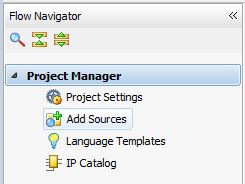
1.Click Add Sources under Project Manager of the Flow Navigator pane.
Add Sources
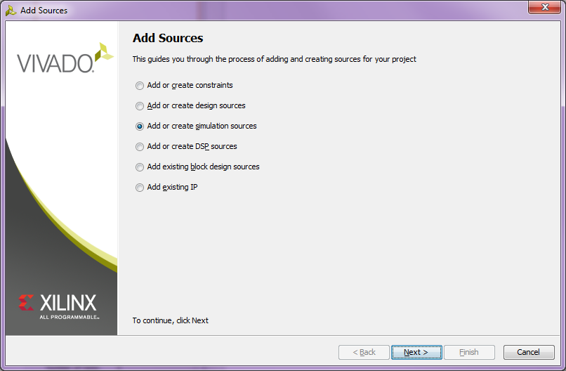
2.Select Add or Create Simulation Sources option and click Next.
Add Source Window
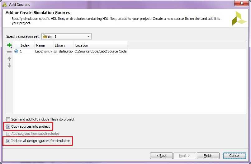
3.In the Add or Create Simulation Sources window, Click the green + symbol and select Add Files,Refer to the directory where you extracted the source code and select file Lab2.sim, Click OK. make sure Copy sources into project is checked and Include all design sources for simulation is checked as well. Click Finish.
Add simulation file
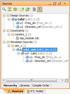
4.Select the Sources pane and expand the Simulation Sources group. Lab2_sim.v file is added under the Simulation Sources group, and Lab2.v is automatically placed in its hierarchy as a UUT instance (uut stands for Unit Under Test).
Sources Pane
5.This step is just to see how Vivado organizes simulation files. Use Windows Explorer, observe that the sim_1 directory is created at the same level as constrs_1 and sources_1 directories under the lab2.srcs directory, and that a copy of lab2_sim.v is placed inside”C:\embeddedcentric\lab2\lab2.srcs\sim_1\imports\Lab2 Source Code”.
6.Back to Vivado. Double click on lab2_sim in the Sources pane to view its contents. The simulation file (aka testbench) instantiates Lab2 design as the unit under test(UUT), in lines 49 till 53.
Lab2 design as a Unit Under Test
The inputs of Lab2 is simulated in line 62.
Input stimuli
Note that the five bits of switches represents the following control signals in this exact order (Down[4],Up[3],Low[2],High[1], Medium[0]). When you assert a one means you activate that specific control signal, therefore 01010 means counts up with high speed of blinking.
The clock simulating Lab2 module is generated using an always block in line 68, the period of this clock is 10 ns. (5×2). The first line in the simulation file ‘timescale 1ns/1ps defines the simulation step size and the resolution , it means any time constant following the # symbol will be considered in nanosecond, and the smallest period of time visible in the simulation is picosecond.
Clock stimulus
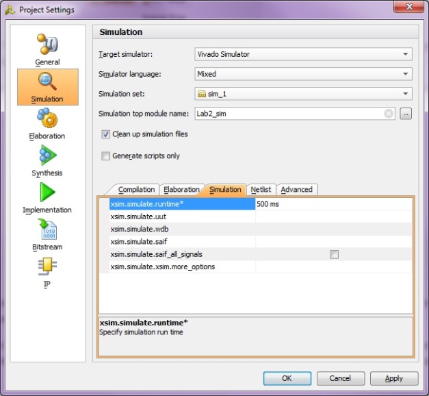
7.Select Simulation Settings under the Project Manager of the Flow Navigator pane. A Project Settings window will appear showing the Simulation properties form.
8.Select Simulation tab, and set Simulation Run Time value to 500 ms( half a second ) and click OK. ( Note: you may need to change the timescale resolution if your machine’s performance is low).
Project Settings Window
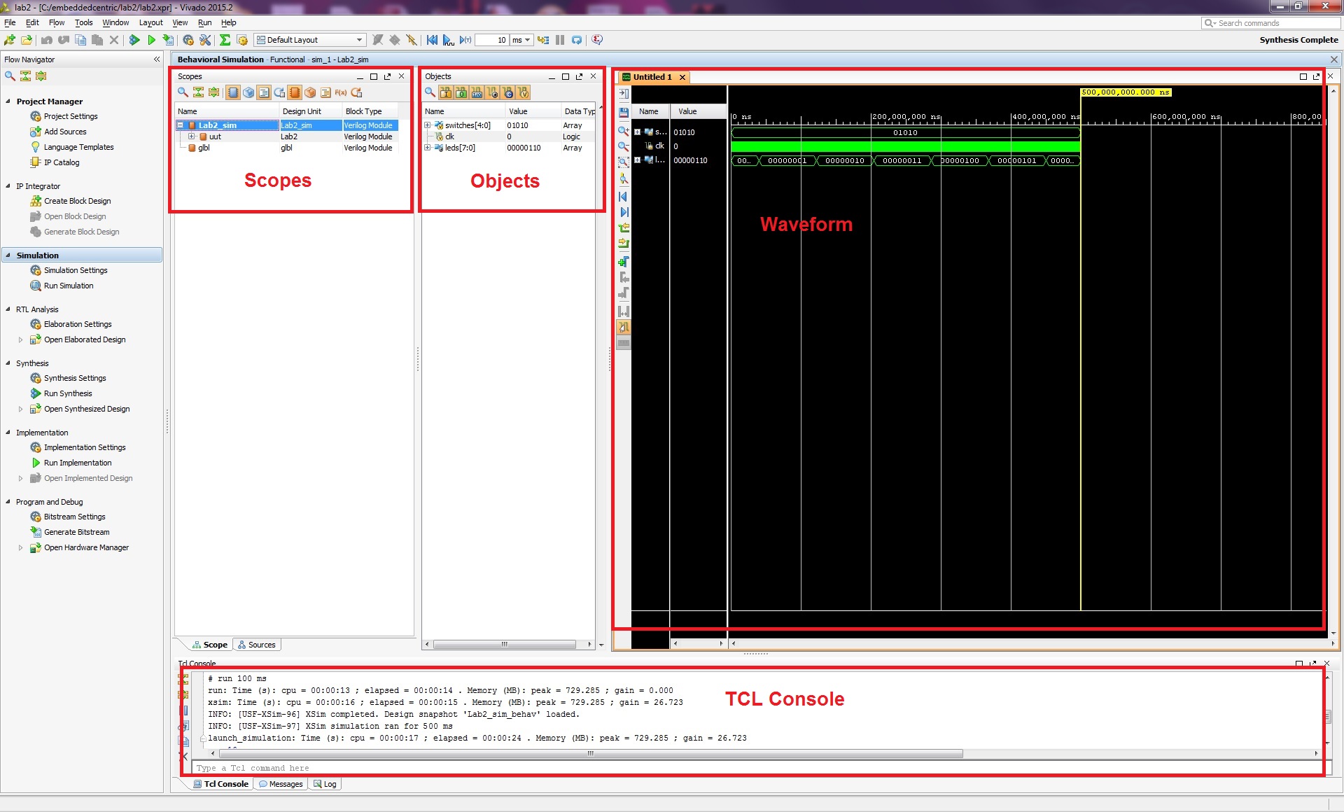
9.Click on Run Simulation > Run Behavioral Simulation under the Project Manager of the Flow Navigator pane. The testbench and source files is compiled and Vivado simulator will be run. You will see a simulation output similar to the one shown below ( Click on the figure to enlarge):
Design Simulation
There are four main views in Vivado Simulator : (i) Scopes: where the testbench hierarchy as well as glbl instances are displayed, (ii) Objects: where top-level signals are displayed, (iii) Waveform: simulation results are displayed there, and(iv) Tcl Console: simulation activities are displayed in text.
By examining the waveform, with (01010) stimuli applied to input by the testbench, the output was actually increasing (started from 0 (00000000)and reached 6(00000110)) in half a second. There were 6 transactions in half a second , i.e. 12 in a second. So we can conclude that the blinking of LEDs would actually happen at a 12Hz frequency (Which is relatively fast for the human eye ,but still we can see the blinking clearly ). Remember that the five bits of switches represents the following control signals in this exact order (Down[4],Up[3],Low[2],High[1], Medium[0]) . so If the stimuli is changed to (01100) and the simulation is rerun, the blinking would be running at a lower frequency.
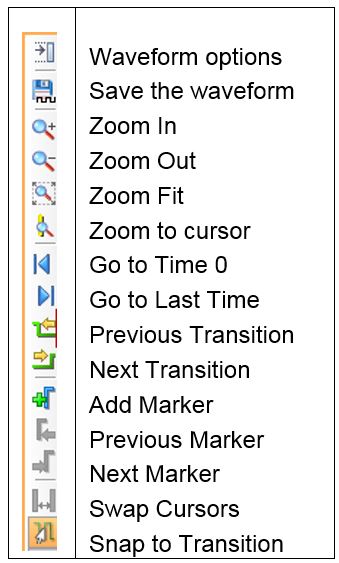
You will see several buttons next to the Waveform window which can be used for the specific purpose as listed in the table below.
Vivado Simulator Features
Click on the![]() pause button to break the simulation and then click on the Zoom Fit button (
pause button to break the simulation and then click on the Zoom Fit button (![]() ) to see the entire waveform. You can also float the simulation waveform window by clicking on the Float button
) to see the entire waveform. You can also float the simulation waveform window by clicking on the Float button![]() on the upper right hand side of the view. This will allow you to have a wider window to view the simulation waveforms. To reintegrate the floating window back into the GUI, simply click on the Dock Window button
on the upper right hand side of the view. This will allow you to have a wider window to view the simulation waveforms. To reintegrate the floating window back into the GUI, simply click on the Dock Window button![]() .
.
you can the change the display format of waves if desired, for instance select “leds [7:0]” in the waveform window, right-click, select Radix, and then select Unsigned Decimal to view the output count as a decimal number instead of binary number .
10.Close the simulator by selecting File > Close Simulation.
11.Click OK and then click No to close it without saving the waveform.
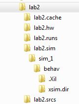
Open the Window Explorer and browse to “C:\embeddedcentric\lab2\lab2.srcs” observe that Vivado has placed newly imported simulation file inside a folder named “sim_1”.
Lab2 directory structure after running simulation
F-Synthesize design and analyze Project Summary report(Post-Synthesis)
1.Click on Run Synthesis under the Synthesis tasks of the Flow Navigator pane. The synthesis process will be run on Lab2.v file (and all its hierarchical files). When the process is completed a Synthesis Completed dialog box with three options will be displayed. Select Open Synthesized Design option and click OK as we want to look at the synthesis results before progressing to the implementation stage.
2.Select the Project Summary tab and spend some time reviewing the information presented there. If you don’t see the Project Summary tab then select Layout > Default Layout, or click the Project Summary icon![]() .
.
Project Summary Post-Synthesis
3.Click on Table tab in Utilization tab. This shows you an estimate of the size of your design in terms of resources of the chip. An interpretation of this table is as follows : Lab2 design uses 48 Flip-Flops (FF) out of the 106400 Flip-Flops available on the Zynq chip(XC7Z020) on the Zedboard. 93 Look up tables ( LUT) , 14 I/O ports ( 5 input +8 output+1 clk) . and 1 Global buffer (BUFG) .
Utilization Post-Synhesis
Note that the Post-Implementation information is empty as we didn’t implement the design yet.
Post-Implementation Utilization empty at this moment
G-Implement the design and analyze the Project Summary output(Post-Implementation).
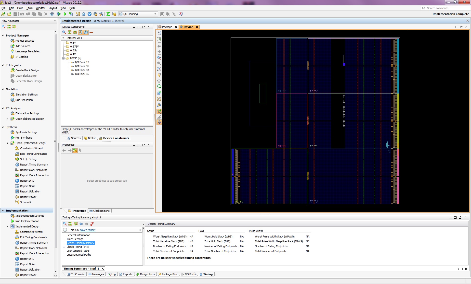
1.Click on Run Implementation under Implementation of the Flow Navigator pane. The implementation process will be run on the synthesized design. When the process is completed an Implementation Completed dialog box with three options will be displayed. Select Open implemented Design and click OK as we want to look at the implemented design in a Device View tab. If a message appears asking you whether you want to close the Synthesized Design click Yes.
Device View(Resources View)
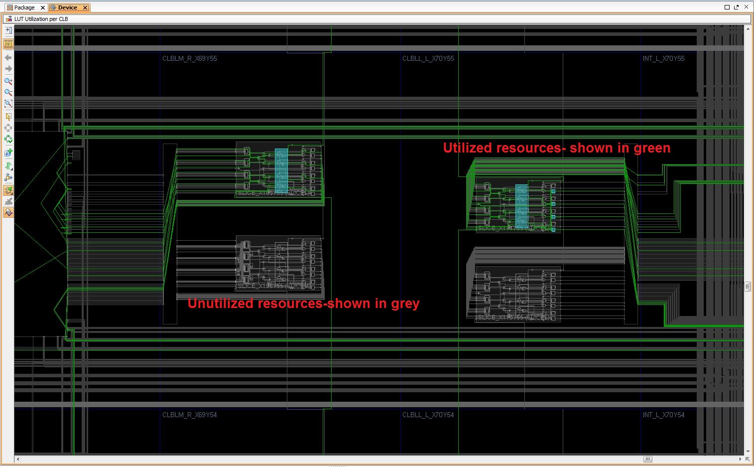
The Device view will show where exactly the design has been placed and how it is routed. You can actually see the LUTs and FFs and other resources of your design. The locations where the circuits are placed and routed affect performance directly, thus Vivado offers high level of flexibility in controlling the place and route process through the Implementation Settings. Timing constraints is one way to insure efficient place and route, however, it is out of the scope of this lab.
By zooming in the Device View you can see the resources in great details. If you click on the show Routing Resources![]() button you can see the wiring and connections between the different components.
button you can see the wiring and connections between the different components.
Zoomed in view of the Device View
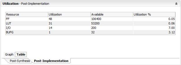
2-Go back to the Project Summary page by clicking on the Project Summary button ![]() and examine the Post-Implementation Utilization. Note that these are the actual utilization of Lab2 Verilog design.
and examine the Post-Implementation Utilization. Note that these are the actual utilization of Lab2 Verilog design.
Post-Implementation Utilization
H-Generate Bitstream and validate functionality
1.Click onGenerate Bitstream entry under the Program and Debug of the Flow Navigator pane.The Bitstream generation process will be run on the implemented design. When the process is completed a Bitstream Generation Completed dialog box with two options will be displayed. Select the Open Hardware Manager option and click OK. The Hardware Manager window will open indicating “unconnected” status.
2.Click on Open Target link, and select Auto Connect ( In case a Firewall message pops up, press Allow Access).
Hardware Manager Tab
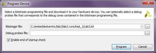
3.Click on Program device , select xc7z020_1. In the next window that pops up leave the default options as is and press Program.
Program Device
The DONE light (Blue LED) on the board will be on when the device is programmed. Verify the functionality of the design on the board by pressing the push buttons on the board, you should observe the same functionality of Lab1.
By this you have completed Lab2-Hardware Design Flow. You can find the complete solution of this lab in here.


