Customized Hardware Integration
In this lab, we will take an inside look on the implementation of an open source customized memory mapped I/O peripheral controller(The Organic LED display controller (ZedboardOLED_V1.0) and its driver). Different aspects of the I/O interface circuitry of the controller is examined, including the control circuits and the data registers. The driver of the controller is reviewed, focusing on the backbone function used to implement it and the role it plays in simplifying the process of interacting with hardware. The ZedboardOLED controller is responsible for initializing the OLED display panel according to the manufacturer’s specifications and instructions. The initialization is archived by sending bursts of bytes (commands) separated by measured time intervals through a SPI interface. After the initialization is complete, the controller provides a processor system access to the OLED display buffer through memory-mapped registers. The controller is a slave AXI-peripheral, with seventeen software-accessed register of 32-bits each, sixteen of which are data registers, while the seventeenth one is for control. The AXI interface is used to connect the controller to any AXI-crossbar compliant processor system. On the other hand, the ZedboardOLED communicates with the OLED display panel through SPI interface. The process of integrating a 3rd party IP is also covered in this lab.

Lab3 Design Flow

Lab3 Block Diagram

Lab3 Board Interface

ZedboardOLED Interface
Background Information
A-OLED Display Panel
The OLED display panel hosted on the Zedboard has 32×128 pixels.The electrical interface of the panel is shown in the figure below:
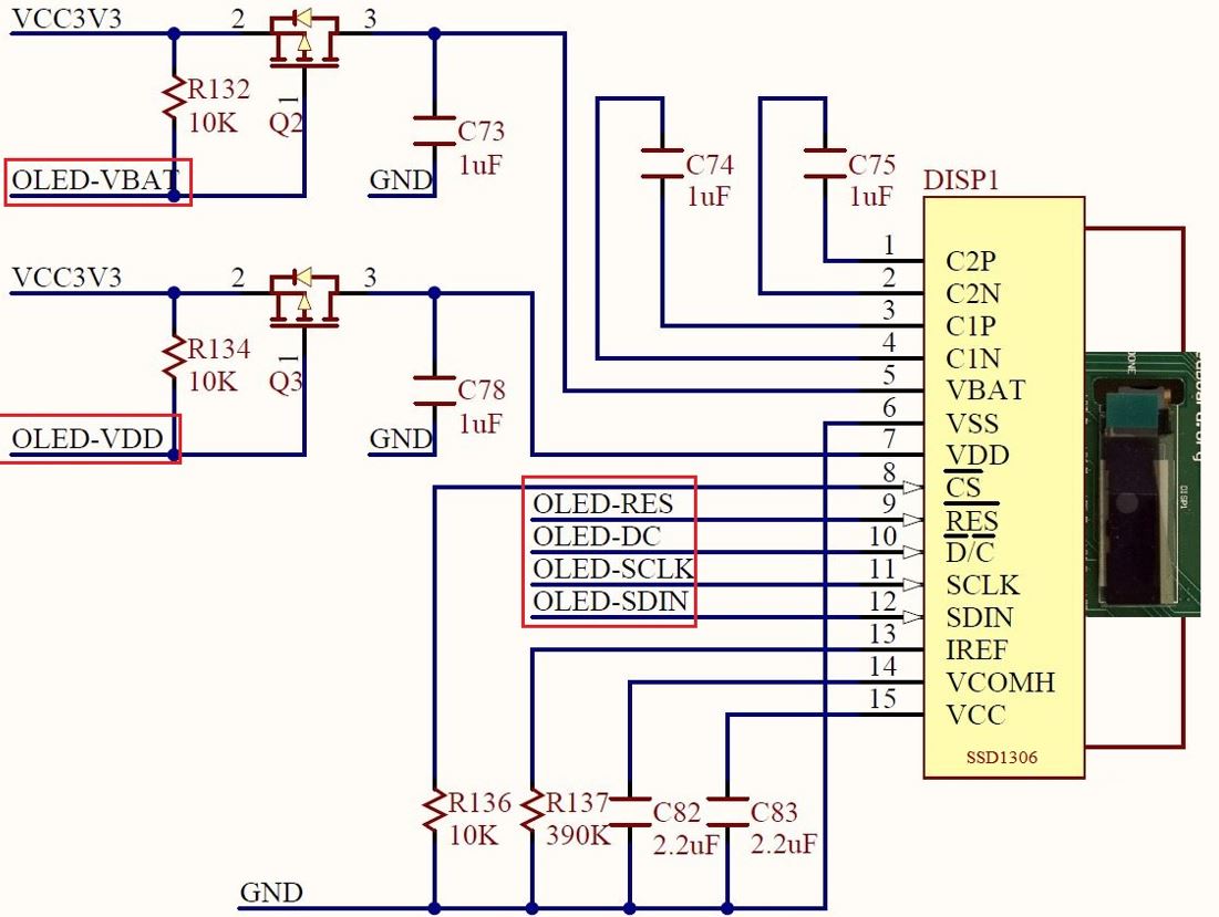
Zedboard OLED Panel Electrical Interface
As we can see from the figure, the OLED panel itself, uses the SSD1306 Segment/Common driver chip by Solomon Systech. It deals with the pixels of the panel directly. It has among other things, a display buffer that holds the bitmaps of the figure to be displayed, as well as, a command register to hold the command being sent over the SPI interface. The SSD1306 interface wiring are summarized in the following table:
| VBAT | Display Voltage Control |
| VDD | Logic Voltage Control |
| DC | Data/Command Control |
| RES | Power Reset |
| SDIN | SPI Data In (MOSI) |
| SCLK | SPI Clock |
The panel has a D/C pin (display or command select) that determines whether bytes sent to the display are interpreted as commands or as display data. The D/C pin is set high for display buffer access and low for command register access. The RES pin is used to reset the SSD1306 display chip. The RES pin is driven low for reset and driven high for normal operation. The low-going reset pulse must be at minimum of 3microseconds in duration for the chip to reset correctly. As we stated previously, the screen is of 32×128 pixels with the physical dimensions illustrated below:

OLED Screen Physical Dimensions
Different shapes can be displayed on the screen by storing different bitmaps in the display buffer (which is named as Graphic Display Data RAM (GDDRAM) in thedatasheet of the SSD1306) . The panel is a serial device that is accessed using Serial Peripheral Interface protocol (SPI) which we will talk about in the next paragraph.
B-SPI Protocol
Data or commands are transferred as bursts of bytes (8-bits) to the panel using the SPI protocol. SPI is commonly used as a method to exchange data between chips on a printed circuit board, and it is usually adopted for short distance, low bandwidth, and single master communication.The master (in our case is the ZedboardOLED Controller- its a master in relation to the SSD1306, however its a slave in relation to the ARM processor) generated a clock (SCLK) and shifts a bit of a data or command on port SDIN on each rising edge of SCLK. On the other hand, the slave ( The OLED panel driver chip –SSD1306) samples every eighth clock and the data byte in the shift register is written to the display buffer or command register in the same clock.

SPI Timing Diagram
C-ZedboardOLED Controller
The responsibilities of ZedboadOLED controller can be summarized by the following points:
1.Implement the AXI-interface(Type: Lite-Slave).
2.Implement the SPI protocol(Type: Master ).
3.Initialize and power-up the screen by following the manufacturer’s instructions.
4.Logically divide the screen into 4 pages, each page can be used to display 16 characters, where each character is represented by 8×8 bitmap.

Logical Division of the OLED Screen
Note: The controller needs to sends 8 bytes of information to the the SSD1306 on the OLED panel side every time it wants to display a character. The sequence followed to send the information is set by the ZedboredOLED controller in column by column order. For instance, if the controller wants to display letter “B” on the screen , it needs to send the following bytes(represented in here in Hexadecimal notation ) in this order: 0x41,0x7F,0x49,0x49,0x49,0x49,0x36,0x00.

Letter B representation in 8×8 bitmap (column by column order)
Characters and symbols in different fonts for different languages, have different bitmaps, check application 8×8 Pixel ROM Font Editor.
![]()
Application 8×8 Pixel ROM
5.Stores the bitmaps of the English alphanumeric on an internal memory to improve performance.
6.Respond to requests made by a processor or a microcontroller implementing the AXI-Interface. These requests could be to display something on the screen or to clear it.
7.Provide seventeen 32-bits software-accessed registers, sixteen of which are data registers, while the seventeenth one is for control. These registers are memory-mapped using the AXI-interface.
The controller is implemented using Verilog, it is a hierarchical design that delegates different functionalities to different blocks, an abstract hierarchical view of the controller is shown below:

ZedboardOLED Hardware Hierarchical Design
In general, the Verilog modules of the controller are implemented as finite state machines(FSM), a brief description of each module is provided here:
SpiCtrl module uses the 100 MHz clock supplied by the PS to generate a 3.125 MHz SCLK (Serial Clock). This module implements the SPI protocol. Every time the ZedboardOLED controller needs to perform a SPI transaction, this module will be involved. It waits until SPI_EN is asserted, active high, and then transitions into the Send state. Then, the module starts shifting out the byte currently held in SPI_DATAto SDO (Serial Data Out) on the rising edge of SCLK. After that, the module transitions into the Done state at which the SPI_FIN signal is pulled high.After that, the module waits for the SPI_EN signal to be de-asserted. At that time, the module transitions into the Idle state and SPI_FIN is pulled low.
Delay module uses the 100 MHz clock supplied by the PS to generate a 1KHz counter which is used to count in milliseconds. This module provides precise timing capabilities for the controller. It waits until DELAY_EN is asserted, active high, and then transitions into the Hold state, then the 1KHz counter starts counting. When the counter reaches the DELAY_MS vector value, the controller then transitions into the Done state at which the DELAY_FIN signal is pulled high.
CharLib is a block memory that contains the bitmaps for the English alphanumeric. The characters are contained in 8 bytes parts(as explained before each character is an 8×8 bitmap). The addressing for this memory is 11 bits and is formatted as followed: (“ASCII Value & “XXX”) where the three bits at the end represent the 8 parts of the character. For instance, the address “01000001001” is the second byte of the character “A”. An important design file associated with the block memory is the CharLib.coe , which is the coefficient file for the block memory. The content of this file will be stored in the block memory inside the controller. The bitmaps of the characters and numbers is saved in locations related to their ASCII code, take a look at how letter “B‟ is saved in the block memory. This should give you an idea on how to add and support new characters and symbols :
The ASCII value of the letter B is “66” . Keep in mind that there is a fixed offset of 3 in the coefficient file due to the heading, therefore, letter B is saved at address (66+3) =69. The 41,7f,49,49,49,49,36,00 are the bitmaps for the letter B stored as 8 bytes in hexadecimal notation.

Bitmap of Letter “B” stored in 8 bytes in hexadecimal notation in CharLib.coe
ZedboardOLED_v1_0_S00_AXI module implements the major functionalities of the controller, including the AXI protocol interface, managing the data registers (slv_reg0-slv_reg15) and the control register (slv_reg16). A finite state machine is used to go through the initialization sequence starting from state Idle, going through 25 initialization states, the initialization sequence ends with the ResetOff state, and then the module enters the WaitRequest state which keeps waiting for a triggers on slv_reg16 control register to initiate an event. The event could be displaying a character on the screen, a string of characters or clearing the screen.
Lastly, the ZedboardOLED_v1_0, this is the top level wrapper for the controller. In this module you find the declarations of the AXI interface ports, as well as the OLED display ports.
D-The Driver
A driver (ZedboardOLED_v1_0) was developed to communicate with the controller, and provide a user friendly interface to the 32×128 organic LED display. The implementation of the driver is in ZedboardOLED.c file. The prototypes of the functions can be found in the header file ZedboardOLED.h. The figure below summarizes the three main functions of the driver :

Driver Functions
It is crucial to emphasize that the data registers (slv_reg0- slv_reg15), and the control register (slv_reg16) of the controller are mapped to the address space, each register is 32 bits in length (4 bytes ), this is why the addresses for these registers are multiple of 4.

Address space of the controller registers
As for the data registers, the ASCII codes of the characters to be displayed on the OLED screen are written in these registers. Each data register is responsible for four characters locations on the screen, as shown in the figure below:

Data Registers and Screen Physical Dimensions Relation
For instance, if slv_reg0 register was filled with the following sequence of bits (01000001 01001100 01001001 01001001 )2 which is equivalent to the decimals 65 76 73 73. The decimals 65 76 73 73 represents the ASCII code for “ALII”.
![]()
slv_reg0 with the content “ALII”
Assuming the D bit of the control register is set high, this will trigger the controller to start bombarding the display buffer of the OLED with the bitmaps of the characters. 256 bits(4x8x8 four characters and each character is a 8×8 bitmap) of data will be sent over the SPI interface to the screen, causing the following message to be displayed on the screen:

OLED Output when slv_reg0 is filled with the bit pattern above
The task of the driver is to simplify the interface to the controller, instead of going through ASCII conversion plus the tedious process of writing these bits individually, and worrying about moving to the position of the next character every time we wanted to display a characters on the screen, the driver can do it on our behalf and simplify our lives.
The driver can do it on our behalf and simplify our lives. The driver backbone function is the Xil_Out32(Address, Value);shipped with the Xilinx Board Support Package(BSP). The Xil_Out32 performs a write operation for a 32-bit memory location by writing the specified Value to the specified Address. Take a look at the code of the print_char() function implemented by the driver

print_char() Function of the ZedboardOLED Driver
Objectives
1.Dive in the low-level implementation details of a memory mapped I/O device controller.
2.Examine the process of transferring technical specifications extracted from hardware component’s datasheets, or from a well-known communication protocols to actual implementations.
3.Understand how software drivers are built. Focusing on their role in simplifying the interaction with hardware.
4.Learn how to integrate new customized hardware (packaged as an IPs) into Vivado Design Suite.
Procedures
A-Create a project in Vivado to target the Zedboard
Follow the same 5 steps in Procedures-A of Lab1. However, in step3 name your project “lab3”.
B-Create an embedded processor project using the IP Integrator
Follow the same 4 steps in Procedures-B of Lab1.
C-Configure the ZYNQ7 Processing System
Follow the same 5 steps in Procedures-C of Lab1.
D-Add the ZedboardOLED IP to Vivado IP repository
Before proceeding with this part, make sure you download the archive file(compressed source code files) of the ZedboardOLED IP core (EmbeddedCentric.com_user_ZedboardOLED_1.0.1) from my GitHub page (Click on the Raw button in order to download the file). After the download is complete, create a new folder on your “C:\” drive and name it “oled_embeddedcentric”. Extract the archive file inside the newly created folder.

ZEDboardOLED source code after extraction
In Vivado, Click on the Project Settings tab available in the Flow Navigator pane. Select IP, then click on the green + symbol in the IP Repositories subview. A browsing window will open up, browse to the location where you extracted the IP core “C:\oled_embeddedcentric” , click Select.

Project Settings Window

Directing to the ZedboardOLED IP
Now, Vivado detects a new IP in this directory, click Apply then OK.

IP Repository After adding ZedboardOLED IP
With this you have added the ZedboardOLED_v1.0 to the IP repository of the current project, the next step is to add it to the block design and connect it to the Zynq processing system from one side, and to the OLED panel from the other side using external ports.
E-Connect the ZedboardOLED IP core
1.Launch the Add IP wizard, and type “oled”. The ZedboardOLED_V1.0 will show up, double click on the IP to add it to the block design.

IP Catalog
2.Notice that the Designer Assistance is available now in the green information bar. It will take care of connecting the IP core to the AXI subsystem of the processing system, configuring the clock and reset, assigning base address (0x43C00000) to the IP, and adding the necessary hardware for the interconnect and synchronization. Click on the Run Connection Automation , leave the default settings as is, and click OK.
The block diagram should look something similar to this:

Block Diagram after running Designer Assistance on the ZedboardOLED
The Designer Assistance has generously done for us the internal connections of the ZedboardOLED IP core. The interface between the ZedboardOLED and the processing system is a well-known protocol (AXI-Lite Slave) for the Designer Assistance to do the connections autonomously,however, it doesn’t know much about the external connections of ZedboardOLED to the OLED display panel, and that is why its still unconnected yet.
Now, we have no other alternative than doing these connections ourselves, Hover the mouse on the ZedboardOLED SDIN port until it changes to a pencil shape, then right click and select Make External. Repeat the same process for (SCLK, DC , RES ,VBAT ,VDD)
ports.

Making external connections to ZedboardOLED manually
3.Right click on any free location on the block diagram and select Regenerate Layout. This will organize the blocks in the design in a neat way. The final layout might look like the one below:
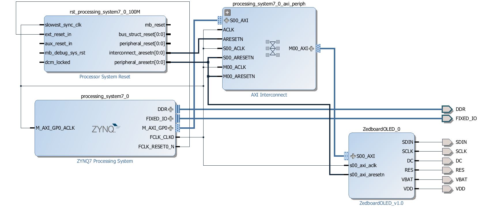
Block Diagram after making external connections
Now we have finished connecting the IP to the processing system through AXI-interface, next step is to connect the external ports we have previously defined of the IP core to the actual Zynq pins hardwired to the OLED panel(the information of these pins are obtained from Zedboard User Manual).
4.In the Flow Navigator window, select Add Sources from the Project Manager section.

Add Sources
The Add Sources dialogue will open. Select Add or Create Constraints.

Add or Create constraints
Click Next, then click on the green + symbol and select Create File

Create a new constraint file
In the next window, Select XDC as the File type and enter oled_constraints as the File name.

Name new constraints file oled_constraints
Click OK, then click Finish in the next window to create the file and close the dialogue.
In the Sources tab, expand the Constraints group and open the newly created XDC file by double clicking on oled_constraints.xdc

Sources pane with oled_constraints selected
Add the following lines to the constraints file, alternatively, they can be copied from the constraints file oled_constraints.xdc available on my GitHub page.
set_property PACKAGE_PIN U10 [get_ports DC]
set_property PACKAGE_PIN U9 [get_ports RES]
set_property PACKAGE_PIN AB12 [get_ports SCLK]
set_property PACKAGE_PIN AA12 [get_ports SDIN]
set_property PACKAGE_PIN U11 [get_ports VBAT]
set_property PACKAGE_PIN U12 [get_ports VDD]
set_property IOSTANDARD LVCMOS33 [get_ports DC]
set_property IOSTANDARD LVCMOS33 [get_ports RES]
set_property IOSTANDARD LVCMOS33 [get_ports SCLK]
set_property IOSTANDARD LVCMOS33 [get_ports SDIN]
set_property IOSTANDARD LVCMOS33 [get_ports VBAT]
set_property IOSTANDARD LVCMOS33 [get_ports VDD]
These physical constraints connects the external ports of the ZedboardOLED IP core to specific pins on the Zynq device. These pins are hardwired to the OLED panel on the Zedboard(Again, the information of these pins are obtained from Zedboard User Manual). Save the constraints file by pressing (Ctrl+S).
5.In the Sources pane, Right click on system.bd and select Create HDL Wrapper to create the top level Verilog file from the block diagram. Select Let Vivado manage wrapper and auto-update when prompted with the next message. Notice that system_wrapper.v got created and placed at the top of the design sources hierarchy.

Create HDL Wrapper
F-Generate Bitstream
In the Program and Debug section in the Flow Navigator pane, click Generate Bitstream. A dialog box will appear to ask you to save the modification you made, click Save .

Generating Bitstream
Generating the Bitstream may take a while to complete, depending on the performance of your machine. After the bitstream generation completes select View Reports in the dialog box, and click OK.
G-Export hardware design to SDK
1.Click File > Export > Export Hardware, make sure you select Include bitstream.
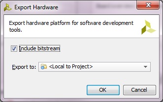
Export Hardware to SDK
2.Select File>Launch SDK. This will open up SDK, notice that all the files related to design including the IP has now been exported to SDK in the previous step, among the resources that got exported is the driver of the ZedboardOLED_v1_0 IP core.
H-Working with SDK
1.In SDK, select File > New > Application Project.
2.In the next window, enter the parameters as provided in the snapshot below:

Application Project oled_test
In the next window, select Empty Application from the available templates and click Finish.
This will compile the BSP and the related drivers.
3.Expand oled_test_bsp>ps7_cortexa9_0>libsrc>zedboardoled_v1_0>src, and examine both ZedboardOLED.c, and ZedboardOLED.h for the driver’s functions.

ZedboardOLED Driver
4.Now we will write a simple application that uses these functions, Expand oled_test directory, right click on the src directory , select New->Source File. In the next window that shows up, type “oled_test.c” in the source file and click Finish.

New Source File
Copy and paste the following C code into the editor view of “oled_test.c”, click Save or hit (Ctrl+S), by doing so, both the oled_test application, and its BSP are compiled automatically and the executable .elf file is generated.
int main(void){
clear_OLED();
print_message(“EmbeddedCentric”,0);
print_message(” ZedboardOLED”,2);
print_message(“By: Ali Aljaani”,3);
return (1);
}
I-Downloading the bitstream and running the application (Hardware verifications)
1.Select Xilinx Tools-> Program FPGA to download the Bitstream (this will take few seconds).
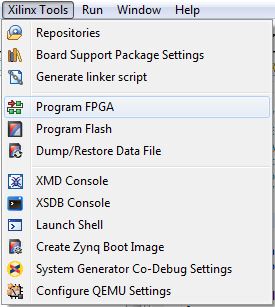
Downloading Bitstream to the PL
2.Select oled_test project directory-> Run As-> Launch on Hardware (GDB) to run the oled_test application on the ARM processor.

Run Application oled_test on the ARM processor
You should see the following message on the OLED screen:

OLED screen output
As you can see, the matter of using the OLED now is simplified by only calling a function and passing it the message that we want to display and its location on the screen. Both the ZedboardOLED controller, and its driver have abstracted the high-level of complexity needed to interact directly with SSD1306 Segment/Common driver of the OLED panel.
By this you have completed Lab3-Customized Hardware Integration. You can find the complete solution of this lab in here.