共发射极放大器的发射极作为输入和输出的参考端。它能够在负载电阻(图中resistor4)上产生一个放大和相反的输出信号。输入信号sinVoltage1通过电容capacitor2耦合到基极,并导致基极电流在其直流偏置附近上下波动。该基极电流的波动相应产生了集电极电流的波动。由于晶体管的电流增益,集电极电流的变化量要远大于基极电流的变化量。这就产生了在集电极电压是一个更大的变化量,并且与基极信号电压反相。集电极电压的这个变化量又被电容耦合 到负载上,产生输出电压。
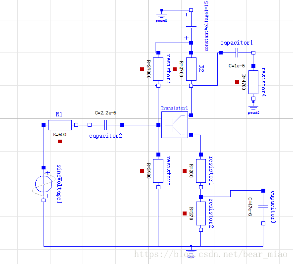
电路
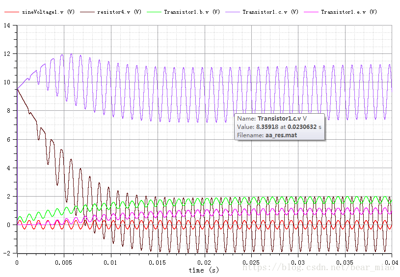
曲线
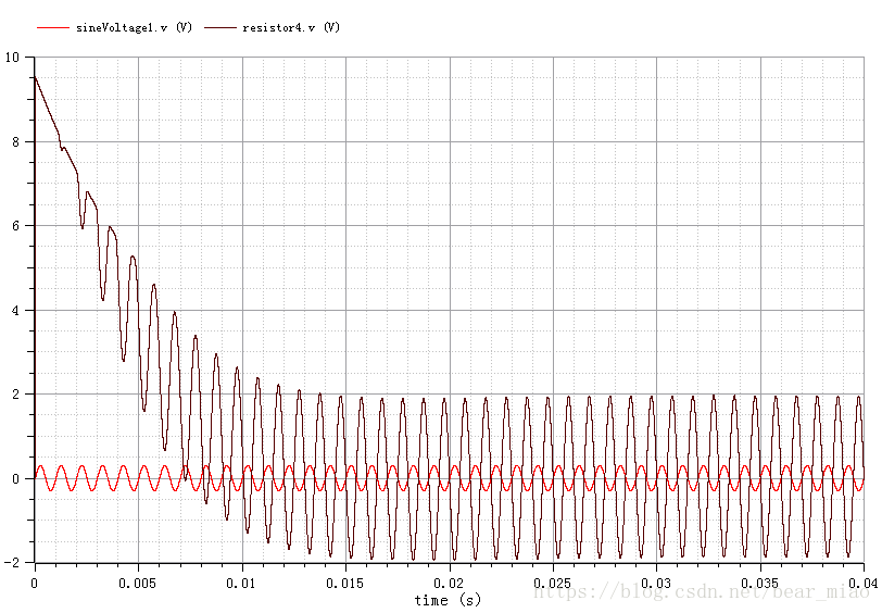
输入和输出曲线(信源频率1000HZ)
程序
model aa "Simple NPN transistor amplifier circuit"
import Modelica.Electrical.Analog.Basic;
import Modelica.Electrical.Analog.Sources;
import Modelica.Electrical.Analog.Examples.Utilities;
import Modelica.Icons;
extends Icons.Example;
Modelica.Electrical.Analog.Basic.Resistor R1(R = 600) annotation(
Placement(visible = true, transformation(extent = {{-64, -14}, {-44, 6}}, rotation = 0)));
Modelica.Electrical.Analog.Basic.Resistor R2(R = 2700) annotation(
Placement(visible = true, transformation(origin = {26, 30}, extent = {{-10, -10}, {10, 10}}, rotation = 270)));
Modelica.Electrical.Analog.Basic.Ground Gnd1 annotation(
Placement(visible = true, transformation(extent = {{21, -88}, {31, -78}}, rotation = 0)));
Modelica.Electrical.Analog.Examples.Utilities.Transistor Transistor1(ct(v(start = 0, fixed = true))) annotation(
Placement(visible = true, transformation(extent = {{6, -14}, {26, 6}}, rotation = 0)));
Modelica.Electrical.Analog.Sources.ConstantVoltage constantVoltage1(V = 15) annotation(
Placement(visible = true, transformation(origin = {26, 56}, extent = {{-10, -10}, {10, 10}}, rotation = 90)));
Modelica.Electrical.Analog.Basic.Resistor resistor1(R = 200) annotation(
Placement(visible = true, transformation(origin = {32, -32}, extent = {{-10, -10}, {10, 10}}, rotation = -90)));
Modelica.Electrical.Analog.Basic.Resistor resistor2(R = 270) annotation(
Placement(visible = true, transformation(origin = {32, -58}, extent = {{-10, -10}, {10, 10}}, rotation = -90)));
Modelica.Electrical.Analog.Basic.Resistor resistor3(R = 27000) annotation(
Placement(visible = true, transformation(origin = {6, 30}, extent = {{-10, -10}, {10, 10}}, rotation = 270)));
Modelica.Electrical.Analog.Basic.Ground ground1 annotation(
Placement(visible = true, transformation(extent = {{3, 56}, {13, 66}}, rotation = 0)));
Modelica.Electrical.Analog.Basic.Capacitor capacitor1(C = 1e-6) annotation(
Placement(visible = true, transformation(origin = {54, 40}, extent = {{-10, -10}, {10, 10}}, rotation = 0)));
Modelica.Electrical.Analog.Basic.Resistor resistor4(R = 4700) annotation(
Placement(visible = true, transformation(origin = {64, 22}, extent = {{-10, -10}, {10, 10}}, rotation = 270)));
Modelica.Electrical.Analog.Basic.Ground ground2 annotation(
Placement(visible = true, transformation(extent = {{59, 0}, {69, 10}}, rotation = 0)));
Modelica.Electrical.Analog.Basic.Resistor resistor5(R = 3900) annotation(
Placement(visible = true, transformation(origin = {6, -32}, extent = {{-10, -10}, {10, 10}}, rotation = 270)));
Modelica.Electrical.Analog.Basic.Capacitor capacitor2(C = 2.2e-6) annotation(
Placement(visible = true, transformation(origin = {-26, -4}, extent = {{-10, -10}, {10, 10}}, rotation = 180)));
Modelica.Electrical.Analog.Sources.SineVoltage sineVoltage1(V = 0.3, freqHz = 1000) annotation(
Placement(visible = true, transformation(origin = {-64, -40}, extent = {{-10, -10}, {10, 10}}, rotation = -90)));
Modelica.Electrical.Analog.Basic.Capacitor capacitor3(C = 47e-6) annotation(
Placement(visible = true, transformation(origin = {70, -54}, extent = {{-10, -10}, {10, 10}}, rotation = -90)));
equation
connect(resistor2.n, Gnd1.p) annotation(
Line(points = {{32, -68}, {32, -78}, {26, -78}, {26, -80}}, color = {0, 0, 255}));
connect(resistor5.n, Gnd1.p) annotation(
Line(points = {{6, -42}, {6, -80}, {26, -80}}, color = {0, 0, 255}));
connect(sineVoltage1.n, Gnd1.p) annotation(
Line(points = {{-64, -50}, {-64, -80}, {26, -80}}, color = {0, 0, 255}));
connect(capacitor3.n, Gnd1.p) annotation(
Line(points = {{70, -64}, {70, -80}, {26, -80}}, color = {0, 0, 255}));
connect(constantVoltage1.n, ground1.p) annotation(
Line(points = {{26, 66}, {17, 66}, {17, 68}, {8, 68}}, color = {0, 0, 255}));
connect(R2.p, constantVoltage1.p) annotation(
Line(points = {{26, 40}, {26, 48}}, color = {0, 0, 255}));
connect(resistor3.p, constantVoltage1.p) annotation(
Line(points = {{4, 40}, {4, 48}, {26, 48}}, color = {0, 0, 255}));
connect(resistor4.n, ground2.p) annotation(
Line(points = {{64, 12}, {64, 8}}, color = {0, 0, 255}));
connect(capacitor2.n, R1.n) annotation(
Line(points = {{-36, -4}, {-44, -4}}, color = {0, 0, 255}));
connect(sineVoltage1.p, R1.p) annotation(
Line(points = {{-64, -30}, {-64, -30}, {-64, -4}, {-64, -4}}, color = {0, 0, 255}));
connect(Transistor1.e, resistor1.p) annotation(
Line(points = {{26, -12}, {32, -12}, {32, -24}, {32, -24}, {32, -24}}, color = {0, 0, 255}));
connect(resistor3.n, Transistor1.b) annotation(
Line(points = {{4, 20}, {6, 20}, {6, -6}}, color = {0, 0, 255}));
connect(resistor5.p, Transistor1.b) annotation(
Line(points = {{6, -22}, {6, -22}, {6, -4}, {6, -4}}, color = {0, 0, 255}));
connect(capacitor2.p, Transistor1.b) annotation(
Line(points = {{-16, -4}, {6, -4}, {6, -4}, {6, -4}}, color = {0, 0, 255}));
connect(R2.n, Transistor1.c) annotation(
Line(points = {{26, 20}, {26, 0}}, color = {0, 0, 255}));
connect(resistor1.n, resistor2.p) annotation(
Line(points = {{32, -44}, {32, -50}}, color = {0, 0, 255}));
connect(capacitor3.p, resistor2.p) annotation(
Line(points = {{70, -44}, {50, -44}, {50, -48}, {32, -48}}, color = {0, 0, 255}));
connect(capacitor1.p, R2.n) annotation(
Line(points = {{44, 40}, {42, 40}, {42, 20}, {26, 20}, {26, 20}}, color = {0, 0, 255}));
connect(resistor4.p, capacitor1.n) annotation(
Line(points = {{64, 32}, {64, 32}, {64, 40}, {64, 40}}, color = {0, 0, 255}));
annotation(
Documentation(info = "<html>
<p>It is a simple NPN transistor amplifier circuit. The voltage difference between R1.p and R3.n is amplified. The output signal is the voltage between R2.n and R4.n. In this example the voltage at V1 is amplified because R3.n is grounded.</p>
<p>The simulation end time should be set to 1e- 8. Please plot the input voltage V1.v, and the output voltages R2.n.v, and R4.n.v.</p>
<p><b>Reference:</b></p>
<p>Tietze, U.; Schenk, Ch.: Halbleiter-Schaltungstechnik. Springer-Verlag Berlin Heidelberg NewYork 1980, p. 59</p>
</html>", revisions = "<html>
<dl>
<dt>
<b>Main Authors:</b>
</dt>
<dd>
Christoph Clauß
<<a href=\"mailto:[email protected]\">[email protected]</a>><br>
André Schneider
<<a href=\"mailto:[email protected]\">[email protected]</a>><br>
Fraunhofer Institute for Integrated Circuits<br>
Design Automation Department<br>
Zeunerstraße 38<br>
D-01069 Dresden
</dd>
</dl>
</html>"),
experiment(StopTime = 0.04, StartTime = 0, Tolerance = 1e-06, Interval = 8e-07),
Diagram(coordinateSystem(preserveAspectRatio = false, initialScale = 0.1)),
uses(Modelica(version = "3.2.2")));
end aa;
注:
输入和输出曲线(信源频率100HZ)
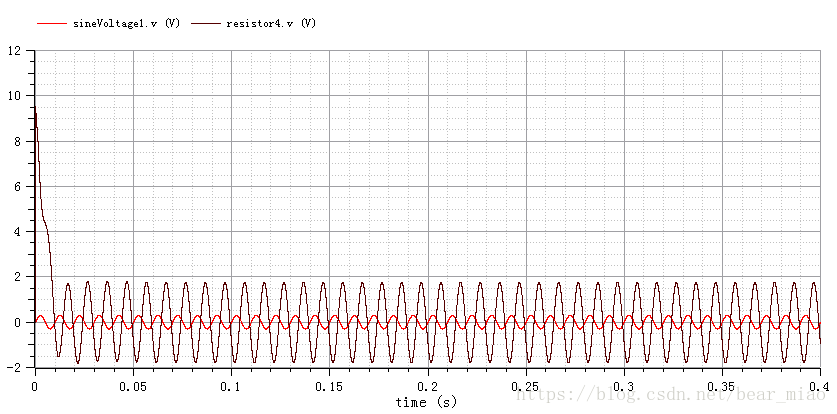
局部图
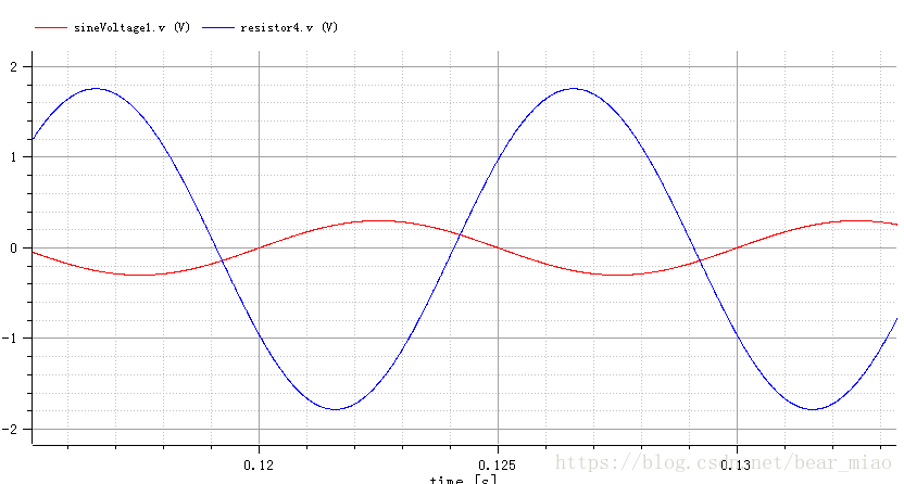
从图中可见,两者相位已经不是刚好反相。
输入和输出曲线(信源频率10HZ)

此时耦合电容的电容值已经不匹配。