| Symbol | Type(DDR视角) | Function | 中文翻译 |
| CK_A CK_An CK_B CK_Bn |
Input | Clock: CK and CKn are differential clock inputs. All address, command, and control input signals are sampled on the crossing of the positive edge of CK and the negative edge of CKn. AC timings for CA parameters are referenced to CK. Each channel (A & B) has its own clock pair. | 时钟:CK和CKn是差分时钟输入。所有地址、命令和控制输入信号都在CK的上升沿和CKn的下降沿交叉采样。CA参数的交流时序参考CK。每个通道(A和B)都有自己的时钟对。 |
| CKE_A CKE_B |
Input | Clock Enable: CKE HIGH activates and CKE LOW deactivates the internal clock circuits, input buffers, and output drivers. Power-saving modes are entered and exited via CKE transitions. CKE is part of the command code. Each channel (A & B) has its own CKE signal. | 时钟使能:CKE高电平激活并且CKE低电平停用内部时钟电路、输入缓冲器和输出驱动器。通过CKE的转换进入和退出省电模式。CKE是命令代码的一部分。每个通道(A和B)都有自己的CKE信号。 |
| CS_A CS_B |
Input | Chip Select: CS is part of the command code. Each channel (A & B) has its own CS signal. | 芯片选择:CS是命令代码的一部分。每个通道(A和B)都有自己的CS信号。 |
| CA[5:0]_A CA[5:0]_B |
Input | Command/Address Inputs: CA signals provide the Command and Address inputs according to the Command Truth Table. Each channel (A&B) has its own CA signals. | 命令/地址输入:CA信号根据命令真值表提供命令和地址输入。每个通道(A和B)都有自己的CA信号。 |
| DMI[1:0]_ADMI[1:0]_B | Input/output | Data Mask Inversion: DMI is a bi-directional signal which is driven HIGH when the data on the data bus is inverted, or driven LOW when the data is in its normal state. Data Inversion can be disabled via a mode register setting. Each byte of data has a DMI signal. Each channel (A & B) has its own DMI signals. This signal is also used along with the DQ signals to provide write data masking information to the DRAM. The DMI pin function - Data Inversion or Data mask - depends on Mode Register setting. | 数据掩码反转:DMI是一个双向信号,当数据总线上的数据被反转时,它被驱动为高电平;当数据处于正常状态时,它被驱动为低电平。可以通过模式寄存器设置禁用数据反转。每个数据字节都有一个DMI信号。每个通道(A和B)都有自己的DMI信号。该信号还与DQ信号一起用于向DRAM提供写数据屏蔽信息。DMI引脚的功能(数据反转或数据屏蔽)取决于模式寄存器的设置。 |
| DQ[15:0]_A DQ[15:0]_B |
Input/output | Data Bus: Bi-direction data bus. | 数据总线:双向数据总线。 |
| DQS[1:0]_A DQS[1:0]_An DQS[1:0]_B DQS[1:0]_Bn |
Input/output | Data Strobe: DQS and DQSn are bi-directional differential output clock signals used to strobe data during a READ or WRITE. The Data Strobe is generated by the DRAM for a READ and is edge-aligned with Data. The Data Strobe is generated by the Memory Controller for a WRITE and must arrive prior to Data. Each byte of data has a Data Strobe signal pair. Each channel (A & B) has its own DQS strobes. | 数据使能:DQS和DQSn是用于在读取或写入期间对数据进行节拍的双向差分输出时钟信号。数据使能由DRAM在读取操作中生成,并与数据边沿对齐。数据使能由内存控制器在写入操作中生成,并且必须在数据之前到达。每个数据字节都有一个数据使能信号对。每个通道(A和B)都有自己的DQS使能信号。 |
| ODT_CA_A ODT_CA_B |
Input | CA ODT Control: The ODT_CA pin is ignored by LPDDR4X devices. ODT-CS/CA/CK function is fully controlled through MR11 and MR22. The ODT_CA pin shall be connected to either VDD2 or VSS. | CA ODT控制:LPDDR4X设备忽略ODT_CA引脚。ODT-CS/CA/CK功能完全通过MR11和MR22进行控制。ODT_CA引脚应连接到VDD2或VSS。 |
| ZQ | Reference | Calibration Reference. Used to calibrate the output drive strength and the termination resistance. There is one ZQ pin per die. The ZQ pin shall be connected to VDDQ through a 240Ω ± 1% resistor. | 校准参考:用于校准输出驱动强度和终端电阻。每个芯片有一个ZQ引脚。ZQ引脚应通过240Ω ± 1%电 |
| VDD1 | Supply | Power Supply 1: Core power supply | 电源供应1:核心电源 dram的core供电的,即dram内部的analog电路 |
| VDD2 | Supply | Power Supply 2: Core power supply | 电源供应2:核心电源 dram的core供电的,即dram内部的analog电路 |
| VDDQ | Supply | DQ Power Supply: Isolated on the die for improved noise immunity. | DQ电源供应:隔离在芯片上,以提高抗干扰能力。 dram的IO上供电的,如DQ/CA等IO的电路,需要的电压比较小 |
| VSS VSSQ |
GND | Ground | 地线 |
| RESETn | Input | Reset: When asserted LOW, the RESETn signal resets both channels of the die. | 复位:当RESETn信号为低电平时,将复位芯片的两个通道。 |
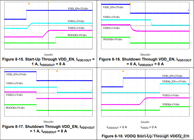
. VDD1 mustramp atthe same time or earlier than VDD2. VDD2 must ramp at the same time or earlier than VDDQ.


抖动的声音:dilo_Abel