版权声明:本文为博主原创文章,未经博主允许不得转载。 https://blog.csdn.net/qq_38204686/article/details/80163202
1.建立


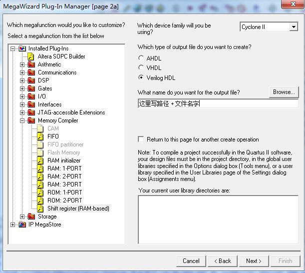
左边选择Shift Register 使用什么芯片 右上就选什么 选择语言 还有工程路径和名字
2.配置
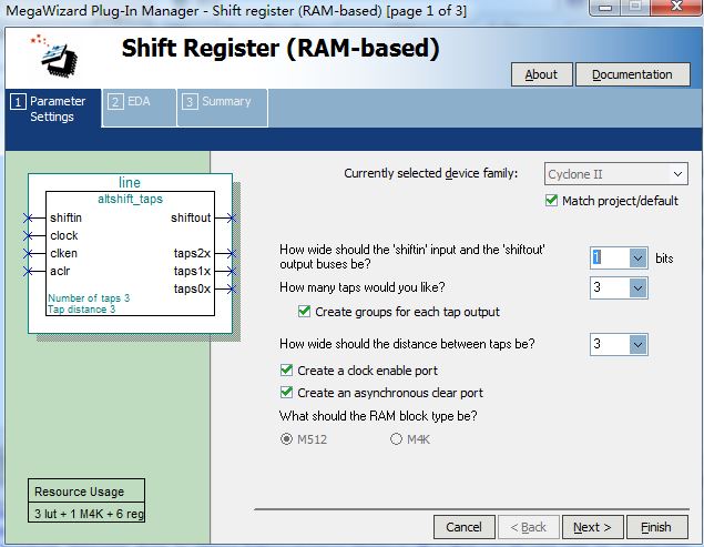
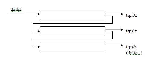
端口 1bit 三个tap 抽头 每个独立分组 每个间距是3 即3X3的一位寄存器
创建时钟使能端口 和 异步清零端口
配置完直接finish就可以
3.仿真调试
1.代码
module cs(
    input clock,
    input aclr,
    input clken,
    input   shiftin,
    output  shiftout,
    output  taps0x,
    output  taps1x,
    output  taps2x
);


line l(
    .clken(clken),
	.clock(clock),
	.aclr(aclr),
	.shiftin(shiftin),
	.shiftout(shiftout),
	.taps0x(taps0x),
	.taps1x(taps1x),
	.taps2x(taps2x)
);

endmodule
2.波形图仿真

aclr是异步复位,只要其为高电平 即复位 如果不需要复位在配置的时候可以不选create这个
clken是使能 其为高电平且 在alcr为低电平的情况下 在clk时钟的上升沿 寄存器移位 不需要也可以不create这个
shifitin 移位寄存器 的输入端 shiftout最终输出端
过程: shiftin -> taps0x -> taps1x -> taps2x(shiftout)