理解FPGA设计需要具体的流程框图,模块化设计。从最基础的计数器设计中,我们可以画个简要的模块。
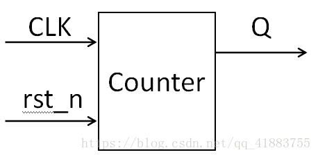
这里的时钟是我们自己定义的,通过控制复位键,我们可以控制计数器模块的运作。
我们需要了解哪些是输入输出端口,这是Verilog设计中的重中之重。
通过模块我们可以知道,clk,rst_n这两个是输入端口,我们定义为input
而输出的Q为输出端口,我们定义为output。
举个例子,我们要设计一个计数到10自动清零的计数器,其Verilog代码如下:
    module counter(
         input clk,rst_n;
         output [3:0] Q;
         always@(posedge clk or negedge rst_n)
       begin
             if(!rst_n)
                  Q<=0;
             else begin
                if(Q<=10)
                     Q<=Q+1;
                else
                     Q<=0;
             end
       end
其testbeach测试代码如下:
`timescale 1ns/1ns
module counter_tb();
     reg clk,rst_n;
     wire [3:0] Q;

     initial begin
     clk=0;
     forever #10 clk=~clk;
     end

     initial begin
     rst_n=0;
     #10 rst_n=1;
     end

 counter u1(
      .clk(clk),
      .rst_n(rst_n),
      .Q(Q));
 endmodule
笔者在起初学习Verilog数字系统设计时,也是很头痛这个计数器,自学了将近两周才明白了FPGA设计的深邃,一定要进行模块化设计,理清输入与输出端口,方能很轻松地设计出自己想要的模块。