强烈建议先看完下面两篇再看这一篇:
FPGA——SPI总线详解(概念)_居安士的博客-CSDN博客_fpga芯片
FPGA——SPI总线控制flash(1)(含代码)_居安士的博客-CSDN博客
在(1)中详细介绍了写使能,读状态,擦除三种操作,接下来介绍如何使用SPI总线对flash进行读写
目录
flash页写
页写指令允许在先前擦除(FFh)的存储器位置编程一个字节到 256个字节(一页)的数据。 在器件接受页写指令(状态寄存器位 WEL=1)之前,必须执行写使能指令。 该指令通过将 /CS 引脚驱动为低电平,然后将指令代码“02h”后跟一个 24 位地址 (A23-A0) 和至少一个数据字节移入 DI 引脚来启动。 当数据被发送到设备时,/CS 引脚必须在指令的整个长度内保持低电平。
页写模块框图如下:

先向fifo写入数据,fifo写完了之后,再从fifo里面读数据(start_write),启动页写操作
首先发送02H的指令,后面是24位数据首地址,后面至多可以跟256个字节(256*8位)的数据
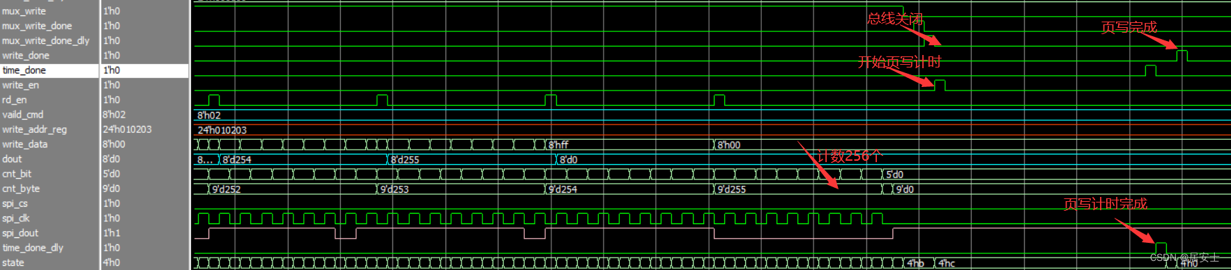
ps:页写需要时间,需要设置定时器,保证页写时间结束之后(3ms)停止页写

输入输出信号:
| 名称 |
输入输出 |
位宽 |
解释 |
| start_write |
input |
1 |
启动页写 |
| brust_length |
input |
9(256个字节) |
突发长度:写入数据的长度 |
| write_addr |
input |
24 |
页写数据24位首地址 |
| clk_wr |
input |
1 |
fifo写入时钟 |
| wr_en |
input |
1 |
fifo写使能信号 |
| din |
input |
8 |
fifo输入数据 |
| wr_fifo_empty |
output |
1 |
fifo空 |
| wr_fifo_full |
ouput |
1 |
fifo满 |
| spi_cs |
output |
1 |
spi片选线 |
| spi_clk |
output |
1 |
spi时钟线 |
| spi_dout |
output |
1 |
spi输出 |
| mux_write |
output |
1 |
写总线请求 |
| mux_write_done |
input |
1 |
写总线应答 |
| write_en |
output |
1 |
启动计时器 |
| time_done |
input |
1 |
计时器完成 |
| write_done |
output |
1 |
页写操作完成 |
flash页写流程图如下:
 页写过程:
页写过程:
0(初始状态):把页写突发长度和页写地址寄存
1(指令解析):把02h给指令寄存器
2(请求总线):请求打开总线
3(发送指令1):把指令最高位给spi_dout,移完8位把地址最高位给spi_dout
4(发送指令2):移位8位指令
5(发送地址1):把地址最高位给spi_dout,移完24位把数据最高位给spi_dout
6(发送地址2):移位24位地址
7(发送数据1):把数据最高位给spi_dout,移完8位把cnt_byte加一;
如果cnt_byte小于突发长度-1,启动fifo读使能
否则,关闭读使能,把下一个字节的数据给spi_dout
8(发送数据2):移位8位数据
9(计数发送数据):判断cnt_byte是否等于突发长度
10(停止):请求总线停止
11(等待总线应答2):等待总线同意停止
12(等待页写时间到):3ms的延时
13(页写完成)
页写代码如下:
module write_top(
input clk              ,
input clk_wr           ,//fifo时钟
input reset            ,
input start_write      ,//启动页写
//fifo部分驱动接口
input [8:0]brust_length,//突发长度
input [23:0]write_addr ,//初始地址
input wr_fifo_en       ,//写使能
input [7:0]din         ,//写数据
output wr_fifo_empty   ,//fifo空
output wr_fifo_full    ,//fifo满
//总线接口
output reg spi_cs      ,//spi片选
output reg spi_clk     ,//spi时钟
output reg spi_dout    ,//spi输出
output reg  mux_write        ,//请求总线
input mux_write_done  ,//总线应答
output reg write_done  ,//页写完成
//计时器
input time_done        ,//计时完成
output reg write_en    //启动计时

    );


    //例化页写延时
    erase_time inst_erase_time(
      .clk      (clk),
      .reset    (reset),
      .write_en (write_en),//页写计时
      .erase_en (),//擦除计时
      .erase_cmd(),//擦除模式选择
      .time_done(time_done)

    );

    //例化FIFO

reg rd_en                 ;//fifo读使能
wire[7:0] dout            ;//fifo输出

  FIFO_wr inst_FIFO_wr (
  .rst(reset),                  // input wire rst
  .wr_clk(clk_wr),            // input wire wr_clk
  .rd_clk(clk),            // input wire rd_clk
  .din(din),                  // input wire [7 : 0] din
  .wr_en(wr_fifo_en),              // input wire wr_en
  .rd_en(rd_en),              // input wire rd_en
  .dout(dout),                // output wire [7 : 0] dout
  .full(wr_fifo_full),                // output wire full
  .empty(wr_fifo_empty),              // output wire empty
  .wr_rst_busy(wr_rst_busy),  // output wire wr_rst_busy
  .rd_rst_busy(rd_rst_busy)  // output wire rd_rst_busy
);


 reg [7:0] vaild_cmd       ;//指令寄存器
 reg [23:0]write_addr_reg  ;//地址寄存器
 reg [7:0] write_data      ;//数据寄存器
 reg [8:0] brust_length_reg;//突发长度寄存器

 reg [4:0] cnt_bit          ;//位计数器
 reg [8:0] cnt_byte         ;//字节计数器

 reg [3:0]state;//定义状态机

always@(posedge clk)begin
	if(reset)begin
		spi_cs          <=1'd1;
    spi_clk         <=1'd0;
    spi_dout        <=1'd1;
    write_done      <=1'd0;
    write_en        <=1'd0;
    vaild_cmd       <=8'd0;
    write_addr_reg  <=24'd0;
    write_data      <=8'd0;
    brust_length_reg<=9'd0;
    cnt_bit         <=5'd0;
    cnt_byte        <=9'd0;
    mux_write       <=1'd0;
    state<=4'd0;

	end
	else begin
		case(state)
			4'd0:begin
				if(start_write)begin
					state<=4'd1;
					write_addr_reg<=write_addr;
					brust_length_reg<=brust_length;
				end
				else begin
					state<=4'd0;
				end
			end
			4'd1:begin
				vaild_cmd<=8'h02;
				state<=4'd2;
			end
			4'd2:begin
				mux_write<=1'd1;
				if(mux_write_done)begin
					state<=4'd3;
					write_en<=1'd1;//启动延时计时
				end
				else begin
					state<=4'd2;
				end
			end
			4'd3:begin
			  if(cnt_bit==5'd8)begin
				  cnt_bit<=5'd0;
          spi_cs<=1'd0;
          spi_clk<=1'd0;
          spi_dout<=write_addr_reg[23];//提前准备好地址
          state<= 4'd6;
        end
         else begin
          cnt_bit<=cnt_bit+5'd1;
          spi_cs<=1'd0;
          spi_clk<=1'd0;
          spi_dout<=vaild_cmd[7];
          state<= 4'd4;
         end
			 end
			4'd4:begin
				state<= 4'd3;
				spi_cs<=1'd0;
        spi_clk<=1'd1;
        vaild_cmd<={vaild_cmd[6:0],vaild_cmd[7]};
			end
			4'd5:begin
				if(cnt_bit==5'd23)begin
					cnt_bit<=5'd0;
          spi_cs<=1'd0;
          spi_clk<=1'd0;
          spi_dout<=write_data[7];//提前准备好数据
          state<= 4'd7;
				end
				else begin
				  cnt_bit<=cnt_bit+5'd1;
          spi_cs<=1'd0;
          spi_clk<=1'd0;
          spi_dout<=write_addr_reg[23];
          state<= 4'd6;
				end
			end
			4'd6:begin
				state<= 4'd5;
				spi_cs<=1'd0;
        spi_clk<=1'd1;
        write_addr_reg<={write_addr_reg[22:0],write_addr_reg[23]};
			end
			4'd7:begin
				if(cnt_bit==5'd7)begin
					cnt_bit<=5'd0;
          cnt_byte<=cnt_byte+9'd1;//字节计数器++
          spi_cs<=1'd0;
          spi_clk<=1'd0;
          spi_dout<=dout[7];//提前准备fifo输出字节最高位
          state<=4'd9 ;
          if(cnt_byte<brust_length_reg-1)begin//是否达到突发长度
          	rd_en<=1'd1;
          	write_data<=dout;//更新fifo输出的字节
          end
          else begin
          	rd_en<=1'd0;
          end
				end
				else begin
					cnt_bit<=cnt_bit+5'd1;
          spi_cs<=1'd0;
          spi_clk<=1'd0;
          spi_dout<=write_data[7];
          state<=4'd8;
				end
			end
			4'd8:begin
					spi_cs<=1'd0;
          spi_clk<=1'd1;
          write_data<={write_data[6:0],write_data[7]};
          state<=4'd7;
			end
			4'd9:begin
				if(cnt_byte==brust_length_reg)begin
					cnt_bit<=5'd0;
					cnt_byte<=9'd0;
					spi_cs<=1'd1;
          spi_clk<=1'd0;
          spi_dout<=1'd1;
          rd_en<=1'd0;
          state<=4'd10;
				end
				else begin
					state<=4'd7;
					spi_cs<=1'd0;
          spi_clk<=1'd1;//clk连续
          write_data<={write_data[6:0],write_data[7]};//最高位已经发送,因此需要移位
				end
			end
			4'd10:begin
				mux_write<=1'd0;
				state<=4'd11;
			end
			4'd11:begin
				if(mux_write_done)begin
					state<=4'd12;
					write_en<=1'd0;
				end
				else begin
					state<=4'd11;
				end
			end
			4'd12:begin
				if(time_done)begin//延时结束
					state<=4'd13;
				end
				else begin
					state<=4'd12;
				end
			end
			4'd13:begin
				write_done<=1'd1;
				state<=4'd0;
			end
		endcase
	end
end


endmodule关于FIFO的操作方法可以看这篇(1条消息) FPGA存储器(FIFO+RAM+ROM)存储实战_居安士的博客-CSDN博客_fpga的存储器资源
TB文件里面完成fifo的写,仿真代码如下:
module TB_write_top(

    );

reg clk			         ;
reg reset            ;
reg start_write      ;//启动页写
reg [8:0]brust_length;//突发长度
reg [23:0]write_addr ;//初始地址
//fifo部分驱动接口
reg clk_wr           ;//fifo时钟
reg wr_fifo_en            ;//写使能
reg [7:0]din         ;//写数据
wire wr_fifo_empty   ;//fifo空
wire wr_fifo_full    ;//fifo满
//总线接口
wire spi_cs      ;//spi片选
wire spi_clk     ;//spi时钟
wire spi_dout    ;//spi输出
wire  mux_write       ;//请求总线
reg mux_write_done    ;//总线应答
wire write_done       ;//页写完成
//计时器
wire time_done         ;//计时完成
wire write_en         ;//启动计时


 write_top inst_write_top(
 .clk 		     (clk)     ,
 .reset       (reset)     ,
 .start_write (start_write)     ,//启动页写
//fifo部分驱动接口
 .brust_length  (brust_length)   ,//突发长度
 .write_addr    (write_addr)   ,//初始地址
 .clk_wr        (clk_wr)   ,//fifo时钟
 .wr_fifo_en         (wr_fifo_en)   ,//写使能
 .din           (din)   ,//写数据
 .wr_fifo_empty (wr_fifo_empty)  ,//fifo空
 .wr_fifo_full  (wr_fifo_full)  ,//fifo满
//总线接口
 .spi_cs          (spi_cs)  ,//spi片选
 .spi_clk         (spi_clk)  ,//spi时钟
 .spi_dout        (spi_dout)  ,//spi输出
 .mux_write       (mux_write)  ,//请求总线
 .mux_write_done  (mux_write_done)  ,//总线应答
 .write_done      (write_done)  ,//页写完成
//计时器
 .time_done (time_done)       ,//计时完成
 .write_en  (write_en)  //启动计时
    );

    initial begin
     clk=0;
     clk_wr=0;
     reset=1;
     start_write <= 1'b0;
     brust_length<= 9'd0;
     write_addr <= 24'd0;

     #1000;
     reset=0;           //复位信号

     #20000;
     start_write <= 1'b1;
     brust_length<= 9'd255;
     write_addr <= 24'h010203;
     #40;
     start_write <= 1'b0;
     brust_length<= 9'd0;
     write_addr <= 24'd0;
    end

    always #20 clk=~clk;
    always #20 clk_wr=~clk_wr;

    //写FIFO
reg [7:0]count_wait;//FIFO复位需要时间
reg [8:0]count_wren;
always @(posedge clk_wr)begin
   if(reset)begin
    count_wait<=8'd0;
    count_wren<=9'd0;
    wr_fifo_en<=1'b0;
    din<=8'd0;
   end
   else if(count_wait <= 8'd20) begin//fifo复位时间到了再进行下面程序
    count_wait<=count_wait+8'd1;
   end
	 else if(count_wren>=9'd255)begin
	  count_wren<=count_wren;
	  wr_fifo_en<=1'b0;  //fifo写使能=0
	  din<=8'd0;//数据清零
	 end
	 else begin
	  count_wren<=count_wren+9'b1;//计数器++
	  wr_fifo_en<=1'b1; //fifo写使能=1
	  din<=din+8'b1; //数据++
	 end
end

	reg [2:0] state;
	always @(posedge clk)begin
	 if(reset)begin
	  state <= 3'd0;
	  mux_write_done<=1'b0;
	 end
	 else begin
	  case (state)
	  3'd0:begin
	   if(mux_write)begin
	    state <= 3'd1;
	    mux_write_done<=1'b1;
	   end
	   else begin
	    state <= 3'd0;
	    mux_write_done<=1'b0;
	   end
	  end
	  3'd1:begin
	   if(!mux_write)begin
	    state <= 3'd2;
	    mux_write_done<=1'b1;
	   end
	   else begin
	    state <= 3'd1;
	    mux_write_done<=1'b0;
	   end
	  end
	  3'd2:begin
	   mux_write_done<=1'b0;
	   state <= 3'd0;
	  end
	  default :state <= 3'd0;
	  endcase
	 end
	end
仿真结果如下:
首先向FIFO的din写入1~255数据

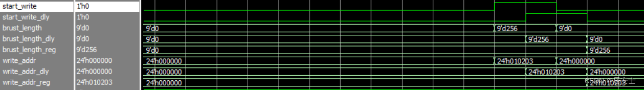
在start_write=1时把突发长度,地址寄存
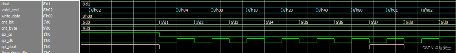
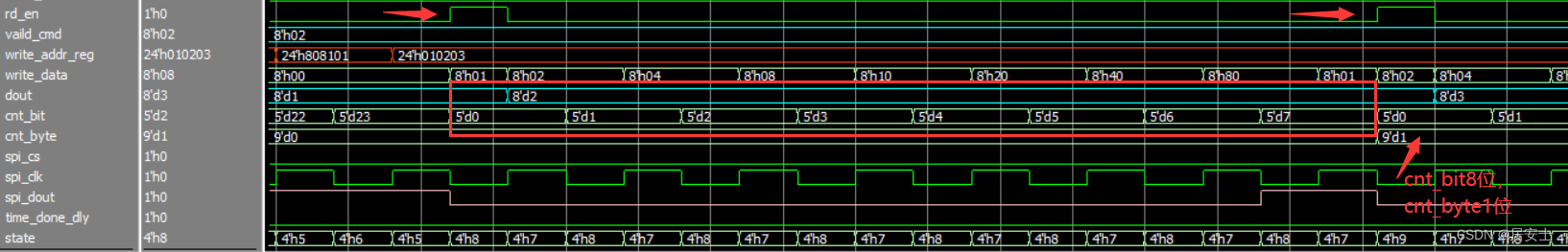
把页写指令移位输出

指令输出完成后,把页写地址移位输出

地址输出完成后,把dout移位输出
flash页读
页读指令(03h)允许从存储器中顺序读取一个或多个数据字节。 该指令通过将 /CS 引脚驱动为低电平,然后将指令代码“03h”后跟一个 24 位地址(A23-A0)移入 DI 引脚来启动。时序如下:
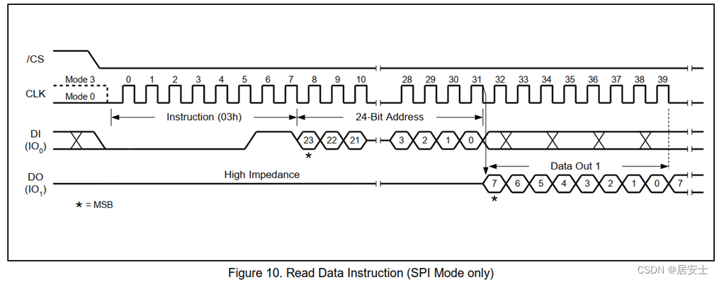
发送完地址之后,总线会输出spi_din数据,高位先发,把总线输出的spi_din缓存到FIFO里
页读模块框图如下:
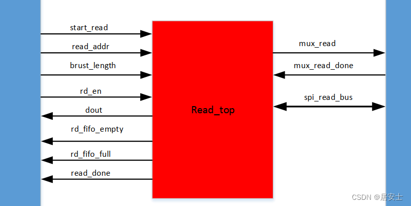
输入输出信号:
| 名称 |
输入/输出 |
位宽 |
解释 |
| start_read |
input |
1 |
开始页读 |
| read_addr |
input |
24 |
读地址 |
| brust_length |
input |
9 |
突发长度 |
| rd_fifo_en |
input |
1 |
fifo读使能 |
| rd_fifo_data |
output |
8 |
fifo读出的数据 |
| rd_fifo_empty |
output |
1 |
fifo空 |
| rd_fifo_full |
output |
1 |
fifo满 |
| spi_cs |
output |
1 |
片选线 |
| spi_clk |
output |
1 |
时钟线 |
| spi_dout |
output |
1 |
spi输出 |
| spi_din |
input |
1 |
spi输入 |
| mux_read |
output |
1 |
请求总线 |
| mux_read_done |
input |
1 |
总线应答 |
| read_done |
output |
1 |
页读完成 |
流程图如下:

0(初始状态):页写启动信号=1时,把读地址和突发长度寄存
1(指令解析):把指令03h输入
2(请求开放总线):请求总线开放,当总线应答后跳转
3(发送指令1):把指令最高位给spi_dout,cnt_bit+1,跳转发送指令2;当cnt_bit==8时,把地址最高位给spi_dout,跳转发送地址2
4(发送指令2):把8位指令进行移位,跳转发送指令1
5(发送地址1):把地址最高位给spi_dout,cnt_bit+1,跳转发送地址2;当cnt_bit==8时,跳转接收2
6(发送指令2):把24位地址进行移位,跳转发送地址1
7(接收1):cnt_bit+1,跳转接收2;当cnt_bit==8,cnt_byte+1,fifo写使能打开,跳转计算模块
8(接收2):把读数据使能打开,跳转接收1
9(计算):判断cnt_byte是否等于突发长度
10(停止页读):请求总线停止
11(请求总线停止):等待总线应答后跳转
12(页读完成):read_done=1
编写代码如下:
module read_top(
input        clk		                ,
input        reset                  ,
input        rd_clk                 ,
input        start_read             ,//开始页读
input [23:0] read_addr              , //页读地址
input [8:0]  brust_length           ,//突发长度
input        rd_fifo_en             ,//fifo读使能
output [7:0] rd_fifo_data           ,//从fifo读出的数据
output       rd_fifo_empty          ,
output       rd_fifo_full           ,
output reg spi_cs                   ,
output reg spi_clk                  ,
output reg spi_dout                 ,
input      spi_din                  ,
output reg mux_read                 ,
input      mux_read_done            ,
output reg read_done

    );
   //例化fifo
    reg wr_en;
    reg [7:0]  valid_data       ;//读出的8位数据

fifo_rd fifo_rd (
  .wr_clk(clk),  // input wire wr_clk
  .rd_clk(rd_clk),  // input wire rd_clk
  .din(valid_data),        // input wire [7 : 0] din
  .wr_en(wr_en),    // input wire wr_en
  .rd_en(rd_fifo_en),    // input wire rd_en
  .dout(rd_fifo_data),      // output wire [7 : 0] dout
  .full(rd_fifo_full),      // output wire full
  .empty(rd_fifo_empty)    // output wire empty
);


reg [7:0]  cnt_bit          ;
reg [7:0]  cnt_byte         ;
reg [7:0]  valid_cmd        ;//页读指令03h
reg [23:0] read_addr_reg    ;//页读地址
reg [8:0]  brust_length_reg ;//突发长度

 //状态机
  reg [4:0] state;

always@(posedge clk)begin
	if(reset)begin
		spi_cs       <=1'd1;
    spi_clk      <=1'd0;
    spi_dout     <=1'd1;
    cnt_bit      <=8'd0;
    cnt_byte     <=8'd0;
    read_done   <=1'd0;
    valid_cmd       <=8'd0  ;
    read_addr_reg   <=24'd0  ;
    brust_length_reg<= 9'd0 ;
		mux_read<=1'd0;
		wr_en<=1'd0;
		valid_data<=8'd0;
    state<=4'd0;
	end
	else begin
		case(state)
			4'd0:begin
				if(start_read)begin
					state<=4'd1;
					read_addr_reg<=read_addr;
					brust_length_reg<=brust_length;
				end
				else begin
					state<=4'd0;
				end
			end
			4'd1:begin
				valid_cmd<=8'h03;
				state<=4'd2;
			end
			4'd2:begin
				 mux_read<=1'd1;
				if(mux_read_done)begin
					state<=4'd3;
				end
				else begin
					state<=4'd2;
				end
			end
			4'd3:begin
				if(cnt_bit==8'd8)begin
					cnt_bit<=8'd0;
					spi_cs       <=1'd0;
   			  spi_clk      <=1'd0;
   			  spi_dout     <=read_addr_reg[23];
   			  state<=4'd6;
				end
				else begin
					cnt_bit<=cnt_bit+8'd1;
					spi_cs       <=1'd0;
   			  spi_clk      <=1'd0;
   			  spi_dout     <=valid_cmd[7];
   			  state<=4'd4;
				end
			end
			4'd4:begin
					spi_cs       <=1'd0;
   			  spi_clk      <=1'd1;
   			  valid_cmd     <={valid_cmd[6:0],valid_cmd[7]};
   			  state<=4'd3;
			end
			4'd5:begin
				if(cnt_bit==8'd23)begin
					cnt_bit<=8'd0;
					spi_cs       <=1'd0;
   			  spi_clk      <=1'd0;
   			  spi_dout     <=1'd1;
   			  state<=4'd7;
				end
				else begin
					cnt_bit<=cnt_bit+8'd1;
					spi_cs       <=1'd0;
   			  spi_clk      <=1'd0;
   			  spi_dout     <=read_addr_reg[23];
   			  state<=4'd6;
				end
			end
			4'd6:begin
					spi_cs       <=1'd0;
   			  spi_clk      <=1'd1;
   			  read_addr_reg     <={read_addr_reg[22:0],read_addr_reg[23]};
   			  state<=4'd5;
			end
			4'd7:begin
				if(cnt_bit==8'd7)begin
					cnt_byte<=cnt_byte+8'd1;
					spi_cs<=1'd0;
          spi_clk<=1'd0;
          cnt_bit<=8'd0;
          wr_en  <=1'd1;//开启写使能,valid_data给fifo的din
					state<=4'd9;
				end
				else begin
					cnt_bit<=cnt_bit+8'd1;
					spi_cs       <=1'd0;
   			  spi_clk      <=1'd0;
   			  state<=4'd8;
				end
			end
			4'd8:begin
					spi_cs       <=1'd0;
   			  spi_clk      <=1'd1;
   			  valid_data<={valid_data[6:0],spi_din};//把总线输出的数据移位进valid_data
   			  state<=4'd7;
			end
			4'd9:begin
				if(cnt_byte==brust_length_reg)begin
					cnt_byte<=8'd0;
					spi_cs<=1'd1;
          spi_clk<=1'd0;
          cnt_bit<=8'd0;
          wr_en  <=1'd0;
					state<=4'd10;
				end
				else begin
					spi_cs<=1'd0;
          spi_clk<=1'd1;
          valid_data<={valid_data[6:0],spi_din};//把总线输出的数据移位进valid_data
          state<=4'd7;
				end
			end
			4'd10:begin
				mux_read<=1'd0;
				state<=4'd11;
			end
			4'd11:begin
				if(mux_read_done)begin
					state<=4'd12;
				end
				else begin
					state<=4'd11;
				end
			end
			4'd12:begin
				read_done   <=1'd0;
   		  state<=4'd0;
			end
		endcase
	end
end

endmodule
编写TB代码:
module TB_read_top(
);
reg clk ;
reg reset ;
reg rd_clk ;
reg start_read ;//开始页读
reg [23:0] read_addr ; //页读地址
reg [8:0] brust_length ;//突发长度
reg rd_fifo_en ;//fifo读使能
wire [7:0] rd_fifo_data ;//从fifo读出的数据
wire rd_fifo_empty ;
wire rd_fifo_full ;
wire spi_cs ;
wire spi_clk ;
wire spi_dout ;
reg spi_din ;
wire mux_read ;
reg mux_read_done ;
wire read_done ;
read_top inst_read_top(
.clk (clk) ,
.reset (reset) ,
.rd_clk (rd_clk) ,
.start_read (start_read) ,//开始页读
.read_addr (read_addr) , //页读地址
.brust_length (brust_length) ,//突发长度
.rd_fifo_en (rd_fifo_en) ,//fifo读使能
.rd_fifo_data (rd_fifo_data) ,//从fifo读出的数据
.rd_fifo_empty (rd_fifo_empty) ,
.rd_fifo_full (rd_fifo_full) ,
.spi_cs (spi_cs) ,
.spi_clk (spi_clk) ,
.spi_dout (spi_dout) ,
.spi_din (spi_din) ,
.mux_read (mux_read) ,
.mux_read_done (mux_read_done) ,
.read_done (read_done)
);
initial begin
clk=0;
rd_clk=0;
reset=1;
start_read<=1'd0;
#100
reset=0;
start_read<=1'd1;
#40
start_read<=1'd0;
end
always #20 clk=~clk;
always #20 rd_clk=~rd_clk;
//状态机
reg [1:0]state;
always@(posedge clk)begin
if(reset)begin
start_read<=1'd0;
read_addr<=24'd0;
brust_length<=9'd0;
spi_din<=1'd0;
state<=2'd0;
end
else begin
spi_din<=~spi_din;
case(state)
2'd0:begin
read_addr<=24'h123456;
brust_length<=9'd10;
if(mux_read)begin
mux_read_done<=1'd1;
state<=2'd1;
end
end
2'd1:begin
if(!mux_read)begin
mux_read_done<=1'd1;
state<=2'd2;
end
end
2'd2:begin
start_read<=1'd0;
read_addr<=24'h0;
brust_length<=9'd0;
state<=2'd3;
end
endcase
end
end
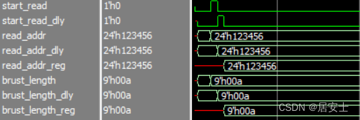
endmodule仿真结果如下:
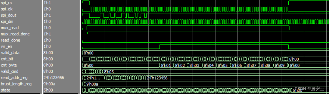
打拍+寄存

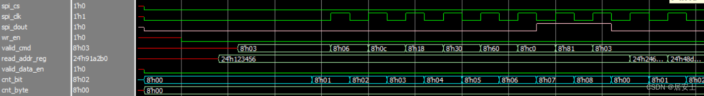
发送指令

发送地址